| |

CMOS FabricationCMOS or Complementary Metal Oxide Semiconductor is a combination of NMOS and PMOS transistors. NMOS is an N-type Metal Oxide Semiconductor, and PMOS is a P-type Metal Oxide Semiconductor. N-type is a type of pentavalent impurities, and P-type is a type of trivalent impurities doped on the semiconductor. The three terminals of the transistors are Gate (G), Source (S), and Drain (D). The doping of p-type/n-type is applied on the D and S terminals. The CMOS transistors are used in various applications, such as amplifiers, switching circuits, logic circuits, Integrated circuit chips, microprocessors, etc. The importance of CMOS in semiconductor technology is its low power dissipation and low operating currents. Its manufacturing requires fewer steps as compared to the Field Effect Transistors and Bipolar Junction transistors. The types of CMOS fabrication are as follows:
Let's discuss the above type of fabrication methods in detail. NMOS FabricationThe doping on the NMOS will be a Pentavalent (five valence electrons) impurity, such as boron and antimony. It has a p-substrate on which the n-type channel is created. As the name implies, the majority carriers participating in the current are electrons. The movement of electrons is fast as compared to the holes. Thus, NMOS is faster than the PMOS. The NMOS fabrication includes eight steps, which are listed as follows: Step 1: Processing the substrateThe first step is to create a p-type substrate. The p-type has trivalent impurities (three valence electrons), such as boron with a concentration upto 1016/cm3. A pure thin film of the silicon wafer is selected on which the p-type impurities are applied as crystals. The diameter of the wafer can be upto 0.15m or 150mm. The chosen wafer material is silicon because it is a clean and high-quality semiconductor material preferred for fabrication. 
Step 2: Silicon dioxide layerSilicon dioxide is made up of two materials silicon (Si) and oxygen (O2). It is also known as oxide. Silicon has a stable structure and is considered as the most abundant metal available on the Earth. It is combined with oxygen that acts as an insulator or conductor under various conditions. 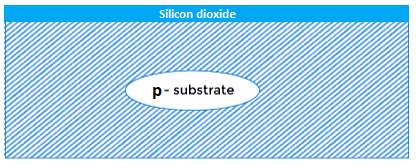
SiO2 layer is grown over the surface of the p-type substrate to prevent it from external factors. It also acts as a barrier to the dopants applied on the layer during the processing. The silicon dioxide thickness is very small, around 0.000001m or 1um. Step 3: Photoresist material is applied on the SiO2 layerThe silicon dioxide layer is covered with the photoresist material. It is a light-sensitive material that forms the coating over the surface of the SiO2 layer. It is useful in reducing the size of the transistors. 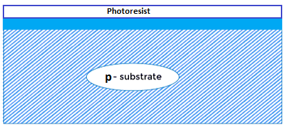
After the photoresist is applied on the silicon dioxide layer, a mask with the desired pattern is used as a medium to expose UV (Ultra-Violet) lights. The UV light through the mask reaches the photoresist material. The exposed resist remains on the surface and the unexposed part is removed from the surface. 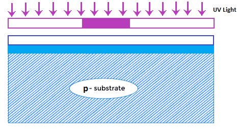
Step 4: Etching the regionsThe unexposed window is removed from the surface and the regions are etched together to form a clean wafer surface. It is shown below: 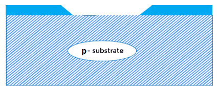
Step 5: Formation of GateThe remaining photoresist layer is removed from the wafer. A thin silicon dioxide layer of 0.0000001m or 0.1 um is grown over the surface. The polysilicon is further added to the surface that forms a gate structure, which is deposited by CVD process. The Chemical Vapor Deposition produces solid materials of high quality. The polysilicon is preferred for the gate because of its high melting point. Its properties are also similar to that of SiO2. Note: The number of doping concentrations, the thickness of the layer, and the resistivity are the three essential elements to be considered for the fabrication process.Step 6: Creating the area for drain and source terminalsThe thin oxide layer on the surface of the silicon wafer is removed and the n-type impurities are inserted with the help of the diffusion process in the specified exposed area. It forms the n-channel at the source and drain terminals. The wafer is first heated at a very high temperature and the gas in passed into it. The area exposed is filled with the gas containing n-type impurities, such as phosphorous. 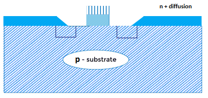
Step 7: SiO2 and photoresist is again deposited on the source and drain terminalsThe same process is again carried to protect the S and D terminals. The oxide layer was removed from the surface of the wafer to create the two terminals, as discussed in step 6. The silicon dioxide and the photoresist are deposited, etched, and masked to protect it. The contact holes are left exposed for the connections. Step 8: Making of the metal layerIt is almost the last step of the NMOS fabrication process. The metal layer of aluminum is deposited on the surface of wafer including the contact holes. The thickness of the aluminum is around 1um. The metal layer is further masked and etched to form the required interconnection pattern. 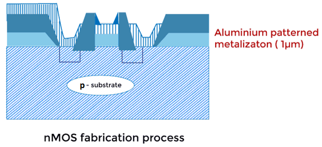
The layer of different materials was applied to the silicon wafer at each step. Thus, the NMOS fabrication process involves the deposition of four major layers. It includes silicon dioxide, photoresist, polysilicon, and the aluminum metal layer. Let's discuss some terms used above in detail. Masking: The masking term was used after the layers SiO2, photoresist, and the aluminum layer. Making is defined as a process of converting the 3D CAD design to the actual layer deposited on a material. It transfers the 3D design to the layer, which is deposited on the surface of the silicon wafer. It is also used to create a pattern on the surface. The CAD (Computer Aided Design) allows the deposition of layers on various wafers with accurate design and length. It is useful in large chip manufacturing processes. Etching: Etching is also used to create a pattern on the substrate or the surface of the wafer. But, it first removes the material from the layer, and creates a pattern from the same material. It enhances the contrast or context of the surface. We know that different layers of SiO2, photoresist, polysilicon, and metal were deposited on the surface of the substrate. The etching process removes the unwanted or extra material from the surface to from holes. The holes can be used for diffusion or for electrical interconnections. N-TUB FabricationIt is a CMOS fabrication process. It means that the PMOS and NMOS are fabricated in different ways. PMOS is created by placing it in the n-well that has a p-type channel. The NMOS is created similarly as discussed above, i.e., on the substrate. Hence, the fabrication of CMOS is known as N-TUB. The steps involved in the N-TUB fabrication process are as follows: 1. WaferThe silicon wafer is selected for doping p-type impurities on it. The doped wafer formed will be the p-type substrate with the trivalent impurities. 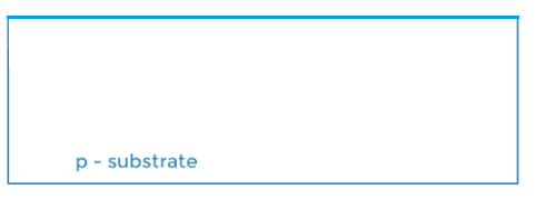
2. Oxidation of waferThe Silicon dioxide layer or oxide layer is created on the surface that protects the substrate. Silicon is one of the metals that are easily available with properties suitable for the fabrication process. 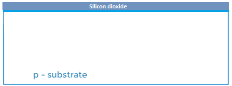
3. Photoresist depositionThe photoresist material is deposited on the wafer. It allows the formation of the n-well on the p-type substrate. 4. N-well MaskThe n-well mask is exposed on the wafer with a particular pattern. The soft part or the unexposed part of the photo resist material is removed to expose the SiO2 layer. 5. Oxide EtchAs discussed, the right part of the wafer is not covered by the photoresist. It is due to the area left for the formation of the n-well. To protect it, the oxide layer is etched with the Hydrofluoric acid. The silicon atoms of the SiO2 layer and the fluoride atoms of HF acid form the strong bond. The silicon wafer is now ready to be exposed to the n-well area. The leftover photoresist material is removed with the help of the etching process. 6. N-well formationThe diffusion process is used to make the n-well on the right side of the wafer. Diffusion is a method of adding impurities from a high concentration region towards a low concentration region. We can also use the ion implantation process to create an n-well. 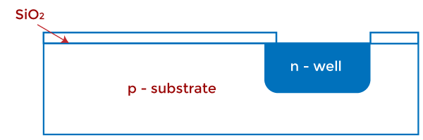
7. Oxide removalThe remaining oxide on the surface of the wafer is stripped off with the help of HF acid. The oxide protects and needs to be removed to create a gate junction. It is done to expose the n-well formed in the above step directly. 
8. Gate formationThe polysilicon is added to the surface that forms a gate structure deposited by CVD process. It is a heavily doped layer of polysilicon present over the thinox, which is a type of thin gate oxide. 9. Poly patterningThe wafer surface is exposed with the photoresist and the mask to create the two G terminals. It is because CMOS is a combination of NMOS and PMOS, and both have separate gates, as shown below: 10. Diffusion patternA protective layer of oxide and photoresist is again applied on the wafer to protect the two gate terminals. 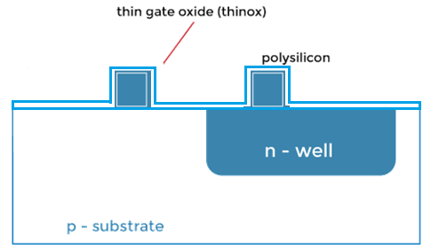
11. Creating area for source and drainTo create the area for S and D, the protective oxide is removed present on the surface of the wafer. It creates the two vacant areas. 12. N-diffusion regionsThe two vacant areas include two source terminals and two drain terminals on each side. The n+ diffusion regions are created by injecting the n+ impurities to those vacant areas. It automatically forms the S and D terminals adjacent to the gate. The n-well on the right side is also created through n+ diffusion. The wafer is heated at a high temperature to create the n-well regions through the diffusion process. 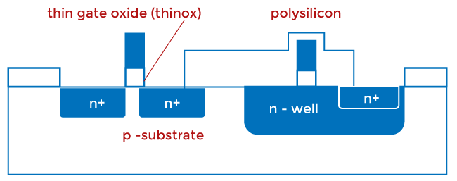
13. P-diffusionThe NMOS has n+ S and D regions, while the PMOS has p+ regions. The n+ regions are already created with the help of above step. Next, the p+ diffusion mask is used that completes the formation of all the active regions of the MOS transistors. 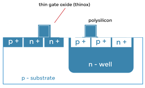
14. Field oxideTo insulate the wafer, the field oxide (SiO2) is deposited on its surface. 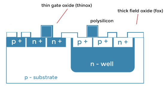
15. Metal formationThe metal layer of aluminum is deposited on the surface of wafer including the contact holes. It also fills the cut holes. It is patterned with the help of metal mask. The entire process of the N-TUB fabrication can be summarized with the help of flow diagram shown below: 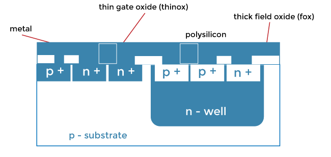
The above process shows the formation of NMOS (left side) and the PMOS transistors. We can also create an inverted circuit fabricated using the same steps. It consists of the PMOS and the NMOS (right side) transistors. The NMOS transistors perform better as compared to PMOS. Thus, n-wells are created to overcome the poor performance of the PMOS. P-TUB FabricationIt is also a CMOS fabrication process. The NMOS transistors are created by placing them in the p-well with a p-type channel. The PMOS is created on the n-type substrate. Hence, the fabrication of NMOS is known as P-TUB. Here, the substrate is n-type, and the doping on the source and drain regions is p-type. A p-well is diffused into the substrate through the diffusion process. The doping concentration and depth of the p-well affect the n-type devices' voltage. Thus, special care is required. The deeper the wells, the larger the surface area it may require. 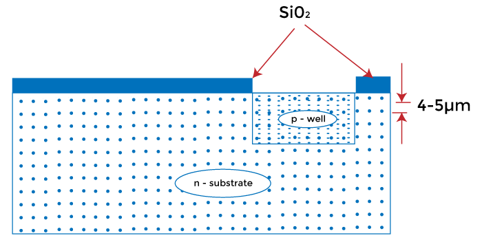
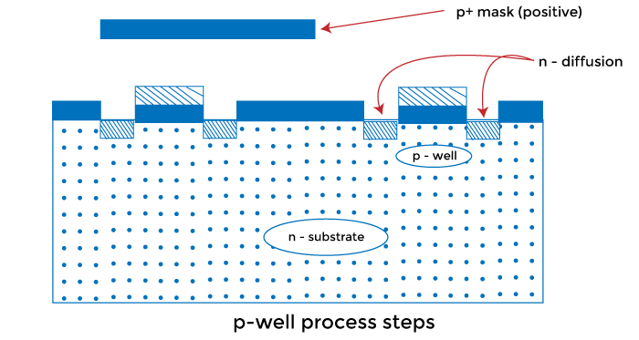
P-TUB combines the PMOS and the NMOS (right side). The n-type acts as a substrate for the PMOS, and the p-well acts as the substrate for the NMOS. These two areas are electrically isolated. The p-well CMOS inverter is shown below: 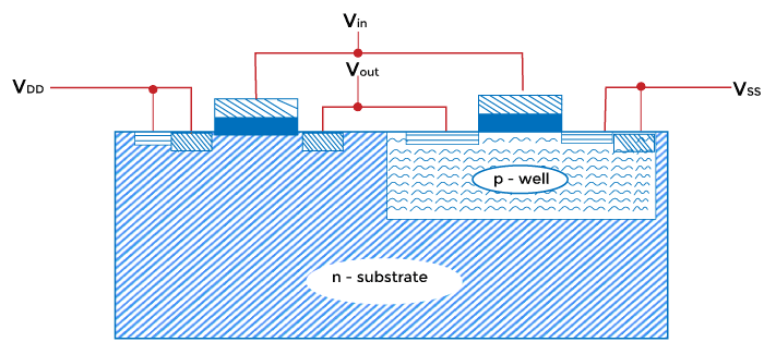
The masking, diffusion, etc. are similar to that of N-TUB. The various mask used in the steps for fabrication are used to defines the areas for deep wells, thick stripped oxide deposition, contacts areas, interconnections, deposition of polysilicon layer, p-diffusions, and metal layer patterns. Twin-TUB FabricationAs the name implies, twin-TUB is a combination of p-well and n-well processes formed on the same substrate. It is also known as dual well process. The high resistivity n-type substrate with both n-well and p-well regions is created, as shown below: 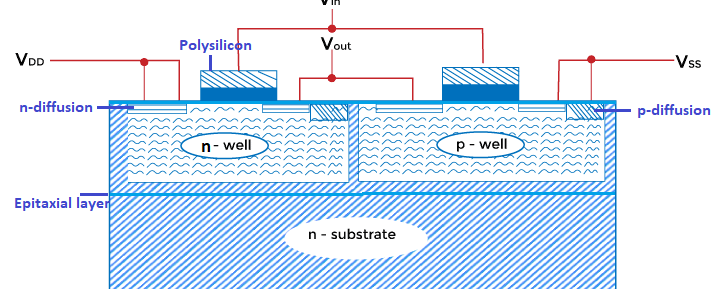
It is an inverting arrangement of twin-tub. The separate transistors and their arrangement help to optimize the n-type devices, p-type devices, and other parameters, such as body effect and threshold voltage. The wafer has two layers. The top layer is the epitaxial layer and the main substrate layer is of n-type. The steps of the twin-TUB fabrication are as follows: Step 1: Deposition of thin oxide layer of silicon dioxide (SiO2). Step 2: The deposition of silicon nitride layer using the CVD process. It has various advantages, such as high temperature stability and light weight. Step 3: The third step includes creating trenches and filling them with SiO2, which is an insulating material. The trenches are created to prevent the current leakage. Step 4: The oxide and nitride is removes to deposit the n-well and p-well regions with the help of diffusion. Step 5: The p-well and the n-well mask are used to dispose of the specific areas on both sides. The implant and annealing are required to adjust the doping concentration of the two wells. The annealing process reduces the hardness for efficient doping. Step 6: A thin layer of SiO2 and polysilicon is applied on the surface of the silicon wafer. Step 7: The source, gate, and drain regions are created using the diffusion process. Step 8: The oxide and nitride layer is again deposited. Step 9: The metal layer of aluminum is deposited on the surface of wafer including the contact holes. It also fills the cut holes. Step 10: A protective glass layer is deposited on the transistor in the last step.
Next TopicCommon base
|
 For Videos Join Our Youtube Channel: Join Now
Feedback
- Send your Feedback to [email protected]
Help Others, Please Share


