| |

What is the Full Form of MOSFETMOSFET: Metal Oxide Semiconductor Field Effect TransistorMOSFET stands for Metal Oxide Semiconductor Field Effect Transistor. It is a field-effect transistor mostly obtained from the regulated oxidation of silicon. It has an isolated gate whose voltage impacts the conductivity of the device. This capacity to modify conductivity in response to the voltage applied can be utilized to enhance or switch electrical signals. MISFET, or metal-insulator-semiconductor field-effect transistor, is practically synonymous with MOSFET. 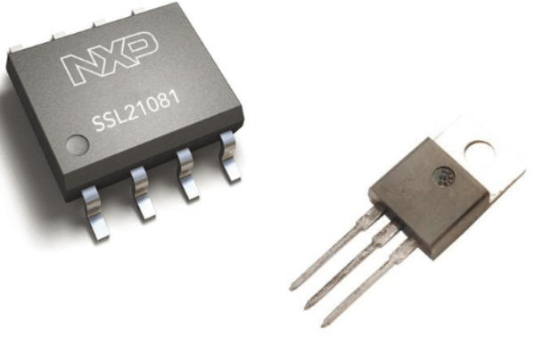
Compared to bipolar transistors, the real benefit of a MOSFET is that it requires essentially minimal input current to regulate the load current. The voltage provided to the gate terminal of an enhancement mode MOSFET enhances the device's conductivity. The voltage supplied at the gate in depletion mode transistors diminishes conductivity. MOSFET's term "METAL" might be misleading because the gate materials are usually made up of a polysilicon layer. Similarly, the term "OXIDE" might be tricky because other dielectric materials are employed to provide strong channels with lower applied voltages. MOSFETs are the most common form of digital circuit transistor, with billions on a memory chip or CPU. They are made with either p-type or n-type semiconductors. Additionally, pairs of MOS transistors can be utilized to construct low-power switching circuits using CMOS logic. When the gate voltage is less than the conductive channel threshold, no conduction occurs between the drain and source, and the switch is turned off. When electrons are attracted by the gate, an n-type conductive channel beneath the oxide is generated, letting electrons move between the n-doped terminals and activating the switch. HistoryIn 1925, Julius Edgar Lilienfeld patented the underlying idea of this type of transistor. William Shockley, John Bardeen, and Walter Houser Brattain suggested the MOS transistor structure during the exploration that eventually resulted in the discovery of the transistor effect. The structure did not have the expected impact due to a surface state problem: traps on the semiconductor surface that kept electrons immobile. Carl Frosch and L. Derick accidentally generated a silicon dioxide layer on a silicon chip in 1955. Further research indicated that silicon dioxide might prevent dopants from diffusing into the piece of silicon. Using this study as a foundation, Mohamed M. Atalla demonstrated that silicon dioxide efficiently solves the problem of one critical class of surface states. Following that, Atalla and Dawon Kahng presented a device like a current MOS transistor in structure. The fundamentals of the device were the same as those used by Bardeen, Shockley, and Brattain in their failed attempt to construct a surface field-effect device. The technology was once considered inferior since it was around 100 times slower than current bipolar transistors. Nonetheless, Kahng highlighted some benefits of the gadget, such as its outstanding simplicity of manufacture and implementation in integrated circuits. What are the compositions in MOSFET? How does it work?Silicon is the most common semiconductor material. Some chip makers, most notably IBM and Intel, have recently begun to use silicon and germanium (SiGe) alloy in MOSFET channels. Unfortunately, several semiconductors with superior electrical characteristics to silicon, such as gallium arsenide, do not form ideal semiconductor-to-insulator contacts and are hence unsuitable for MOSFETs. On additional semiconductor materials, research is being conducted to develop insulators with good electrical properties. To compensate for the increase in power consumption caused by gate current leakage, a high-dielectric is employed as the gate insulator instead of silicon dioxide, and metal gates replace polysilicon (e.g. Intel, 2009). A thin insulating layer, originally of silicon dioxide and, subsequently, silicon oxynitride, separates the gate from the channel. Some companies have introduced a high-dielectric and metal gate pairing at the 45-nanometer node. The electric field penetrates the oxide when a voltage is supplied between the gate and body terminals. At the semiconductor-insulator interface, it forms an inversion layer or channel. The inversion layer creates the circulating current stream between the source and drain. This layer's conductivity is controlled by altering the voltage between the gate and the body. Consequently, it regulates the flow of electricity between the drain and the source. All of that is referred to as enhancement mode.
Next TopicFull Form
|
 For Videos Join Our Youtube Channel: Join Now
Feedback
- Send your Feedback to [email protected]
Help Others, Please Share


