| |

ASIC Design FlowA typical design flow follows the below structure and can be broken down into multiple steps. Some of these phases happen in parallel and some in sequentially. 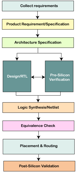
RequirementsA customer of a semiconductor firm is typically some other company who plans to use the chip in its systems or end products. So, the customer's requirements also play an important role in deciding how the chip should be designed. The first step is to collect the requirements, estimate the end product's market value, and evaluate the number of resources required to do the project. SpecificationsThe next step is to collect specifications that describe the functionality, interface abstractly, and over all architecture of the chip to be designed. This can be something along the lines such as:
ArchitectureNow, the architect gives a system-level view of how the chip should operate. They will decide what all other components are required, what clock frequencies they should run, and how to target power and performance requirements. They also decide on how the data should flow inside the chip. An example would be the data flow when a processor fetches imaging data from the system ram and executes them. Meanwhile, the graphics engine will execute post-processed data from the previous batch dumped into another part of memory and so on. 
Digital DesignBecause of the complex nature of modern chips, it's impossible to build something from scratch, and in many cases, many components will be reused. For example, company A requires a FlexCAN module to interact with other modules in an automobile. They can either buy the FlexCAN design from another company to save time and effort or spend resources to build one. It's not practical to design such a system from basic building blocks such as flip-flops and CMOS transistors. Instead, a behavioral description is developed to analyze the design in terms of functionality, performance, and other high-level issues using a Hardware Description Language such as Verilog or VHDL. This is usually done by a digital designer and is similar to a high-level computer programmer equipped with digital electronics skills. VerificationOnce the RTL design is ready, it needs to be verified for functional correctness. For example, a DSP processor is expected to issue bus transactions with fetching instructions from memory and know that this will happen as expected. The functional verification is required at this point, which is done with EDA simulators' help that can model the design and apply a different stimulus to it. This is the job of a pre-silicon verification engineer. 
To save time and reach functional closure, both the design and verification teams operate in parallel, where the designers release an RTL version. The verification team develops a testbench environment and test cases to test the functionality of that RTL version. If any of these tests fail, it might indicate a problem with the design, and a "bug" will be raised on that design element. This bug will have to be fixed in the next version of the RTL release from the design team. This process goes on until there is a good level of confidence in the design's functional correctness. Logic SynthesisNow we will convert this design into hardware schematic with real elements such as combinational gates and flip-flops. This step is called synthesis. Logic synthesis tools enable the conversion of RTL description in HDL to a gate-level netlist. This netlist is a description of the circuit in terms of gates and connections between them. Logic synthesis tools ensure that the netlist meets timing, area, and power specifications. Typically, they have access to different technology node processes and digital elements libraries and can make intelligent calculations to meet all these different criteria. These libraries are obtained from semiconductor fabs that provide data characteristics for different components such as rise or fall times for flip-flops, input-output time for combinational gates, etc. Logic EquivalenceThe gate-level netlist is checked for logical equivalence with the RTL. Sometimes, a gate-level verification is performed where verification of certain elements is done once again, the difference being this time it is at the gate level and a lower level of abstraction. Simulation times tend to be slower because of the huge number of elements involved in the design and back annotated delay information. Placement and RoutingThen, the netlist is inputted to the physical design flow, where automatic place and the route are done with EDA tools' help. The Cadence Encounter and Synopsys IC Compiler are good examples of these kinds of tools. This will select and place standard cells into rows, define ball maps for input and output, create different metal layers, and place buffers to meet timing. Once this process is done, a layout is generated and usually sent for fabrication. This stage is usually handled by the physical design team, who are well familiar with the technology node and physical implementation details. ValidationA sample chip will be made-up either by the same semiconductor firm or sent to a third-party such as TSMC or Global Foundries. This sample now goes through a post-silicon validation process where another team of engineers runs different tester patterns. It is more difficult to debug in post-silicon validation than pre-silicon verification simply because the level of visibility into a chip's internal nodes is drastically reduced. A million clock cycles would have finished in a second, and tracing back to the exact time of error will be time-consuming. If there are any real issues or design bugs found at this stage, this will have to be fixed in RTL, re-verified, and all the steps that follow this will have to be performed. Even though there are multiple steps in the design flow, a lot of the design activity is usually concentrated on the optimization and verification of the RTL description of the circuit. It is important to note that although EDA tools are available to automate the processes, improper usage will lead to inefficient designs. Hence, a designer has to make conscious choices during the design process.
Next TopicDesign Abstraction Layers
|
 For Videos Join Our Youtube Channel: Join Now
Feedback
- Send your Feedback to [email protected]
Help Others, Please Share


