| |

Design Abstraction LayersThe Verilog language would be essential to understand the different layers of abstraction in chip design. The top layer is the system-level architecture that defines the various sub-blocks and groups them based on functionality. For example, a processor cluster can have multiple cache blocks, cores, and cache coherence logic. All of this will be represented as a single block with input and output signals. 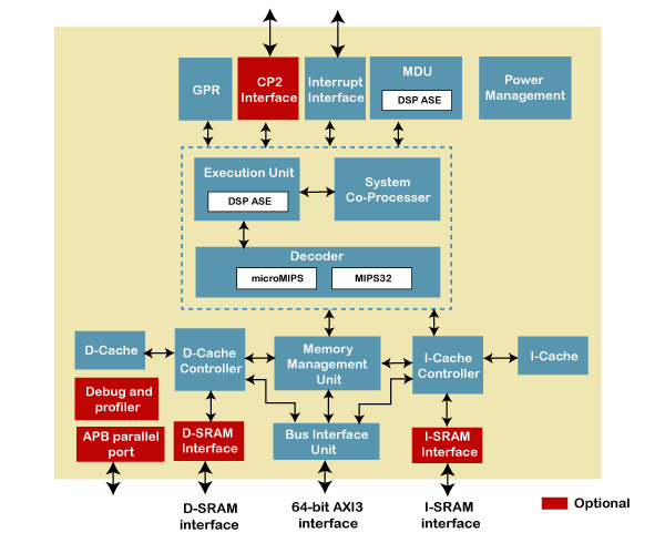
On the next level, each sub-block is written in a hardware description language to describe each block's functionality accurately. Lower level implementation details such as circuit schematics, technology libraries are ignored at this stage. For example, a controller block will have multiple Verilog files, each describing a smaller functionality component. HDLs are then converted to gate-level schematics that involve technology libraries that characterize digital elements such as flip-flops. For example, the digital circuit for a D latch contains NAND gates arranged in a certain manner such that all combinations of D and E inputs produce an output Q given by the truth table. 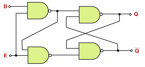
A truth table essentially gives permutation of all input signal levels and the resulting output level. The hardware schematic can also be derived from the truth table using K-maps and Boolean logic. However, it is not useful to follow this method for more complex digital blocks like controllers and processors. 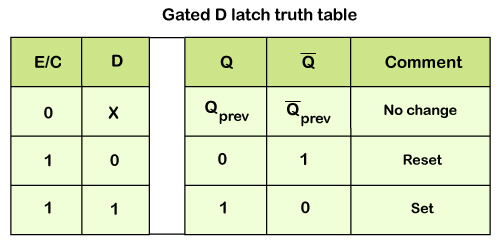
Implementation of a NAND gate is done by the connection of CMOS transistors in a particular format. At this level, the transistor channel widths, Vdd, and the ability to drive the output capacitative load are taken into account during the design process. 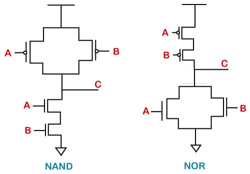
The final step is the layout of these transistors in silicon using EDA tools to be fabricated. Some device and technology knowledge would be required at this level because different layouts end up having different physical properties like resistance and capacitance, among other implications. Design StylesThere are primarily two styles followed in the design of digital blocks, one is top-down, and another is bottom-up methodologies. 1. Top-Down Similarly, each sub-blocks is further divided into smaller components, and the process continues until we reach the leaf cell or a stage where it can't be further divided. 2. Bottom-up We can also use the combination of both flows. Architects define the system-level view of the design, and designers implement each of the functional blocks' logic and get synthesized into gates. A top-down style is followed until this point. However, these gates have been built by following a bottom-up flow, starting with the smallest block's physical layout in the best possible area, power, and performance. These standard cells also have a hardware schematic. And these can be used to obtain various information such as rise and fall in power, times, and other delays. These cells are made available to the synthesis tool, which picks and instantiates them where required.
Next TopicVerilog Data Types
|
 For Videos Join Our Youtube Channel: Join Now
Feedback
- Send your Feedback to [email protected]
Help Others, Please Share


