| |

Verilog Full AdderThe full adder is a digital component that performs three numbers an implemented using the logic gates. It is the main component inside an ALU of a processor and is used to increment addresses, table indices, buffer pointers, and other places where addition is required. A one-bit full adder adds three one-bit binary numbers, two input bits, one carry bit, and outputs a sum and a carry bit. A full adder is formed by using two half adders and ORing their final outputs. A half adder adds two binary numbers. The full adder is a combinational circuit so that it can be modeled in Verilog language. The logical expression for the two outputs sum and carry are given below. A, B are the input variables for two-bit binary numbers, Cin is the carry input, and Cout is the output variables for Sum and Carry. 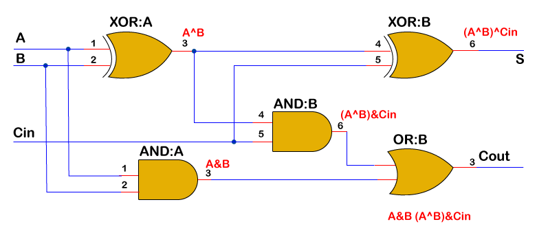
Truth Table
Example An example of a 4-bit adder is shown below, which accepts two binary numbers through the signals a and b. An adder is a combinational circuit. Therefore Verilog can model it using a continuous assignment with assign or an always block with a sensitivity list that comprises all inputs. Below code shows the uses an always block which gets executed whenever any of its inputs change value. Hardware Schematic 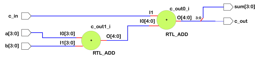
Testbench First, add the timescale directive. It starts with a grave accent ` but does not end with a semicolon. Timescale directive is used for specifying the unit of time used in further modules and the time resolution (one picosecond). The time resolution is the precision factor that determines the degree of accuracy of the time unit in the modules. Next are the module and variable declaration.
Then comes the module instantiation.
The different thing is the use of two system tasks:
When a and b add up to give a number more than 4 bits wide, the sum rolls over to zero and c_out becomes 1. For example, the line highlighted in yellow adds up to give 0x11 and the lower 4 bits get assigned to sum and bit#4 to c_out.
Next TopicPriority Encoder
|
 For Videos Join Our Youtube Channel: Join Now
Feedback
- Send your Feedback to [email protected]
Help Others, Please Share


