| |

T Flip FlopT stands for ("toggle") flip-flop to avoid an intermediate state in SR flip-flop. We should provide only one input to the flip-flop called Trigger input Toggle input to avoid an intermediate state occurrence. Then the flip - flop acts as a Toggle switch. The next output state is changed with the complement of the present state output. This process is known as Toggling. We can construct the T flip-flop by making changes in the JK flip-flop. The T flip-flop has only one input, which is constructed by connecting the input of JK flip-flop. This single input is called T. The Block diagram of the T flip-flop is given below where T defines the "Toggle" input, and CLK defines the "clock signal" input. 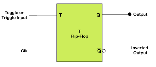
T Flip Flop CircuitThere are two methods which are used to form the T flip-flop:
ConstructionThe T flip-flop is designed bypassing the AND gate's output as input to the NOR gate of the SR flip-flop. The inputs of the "AND" gates, the present output state Q, and its complement Q' are sent back to each AND gate. The toggle input is passed to the AND gates as input. These gates are connected to the Clock (CLK) signal. In the T flip-flop, a pulse train of little triggers is passed as the toggle input, which changes the flip flop's output state. The circuit diagram of the T flip flop using SR flip flop is given below: 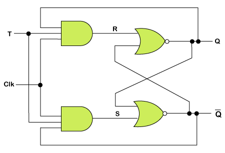
The T flip flop is formed using the D flip flop. In D flip flop, the output after performing the XOR operation of the T input with the output "QPREV" is passed as the D input. The logical circuit of the T flip flop by using the D flip flop is given below: 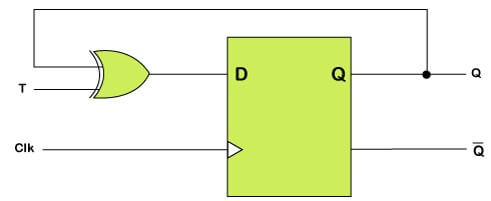
The simplest construction of a D flip flop is with JK flip flop. Both the JK flip flop inputs are connected as a single input T. Below is the logical circuit of the T flip flop, which is formed from the JK flip flop: 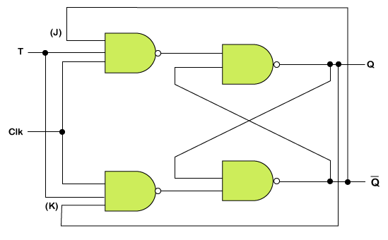
Truth Table of T flip flop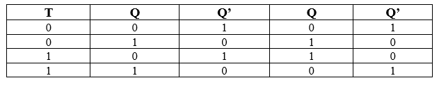
The upper NAND gate is enabled, and the lower NAND gate is disabled when the output Q To is set to 0. Make the flip flop in "set state (Q=1)", the trigger passes the S input in the flip flop. The upper NAND gate is disabled, and the lower NAND gate is enabled when the output Q is set to 1. The trigger passes the R input in the flip flop to make the flip flop in the "reset state (Q=0)". Operations of T-Flip FlopThe T flip flop's next sate is similar to the current state when the T input is set to false or 0.
The next state of the flip flop is opposite to the current state when the toggle input is set to 1.
The T flip flop is toggled when the incoming trigger alternatively changes the set and reset inputs. The T flip flop requires two triggers to complete a full cycle of the output waveform. The frequency of the output produced by the T flip flop is half of the input frequency. The T flip flop works as the "Frequency Divider Circuit." In T flip flop, the state at an applied trigger pulse is defined only when the previous state is defined. It is the main drawback of the T flip flop. The T flip flop can be designed from "JK Flip Flop", "SR Flip Flop", and "D Flip Flop" because the T flip flop is not available as ICs. The block diagram of T flip flop using "JK Flip Flop" is given below: 
ExampleTestbench
Next TopicVerilog D Latch
|
 For Videos Join Our Youtube Channel: Join Now
Feedback
- Send your Feedback to [email protected]
Help Others, Please Share


