| |

Difference between SEM and TEMHigh-resolution images can be obtained using electron microscopy in various fields, such as biomedical research, forensics, and technology. Light microscopes cannot capture images with the same level of detail as electron microscopes, adding information that would otherwise be impossible. 
Every electron microscope operates by directing a stream of focussed electrons in a vacuum toward a sample. Like optical microscopes utilize light to take photos, an electron beam's interaction with the object creates an image for electron microscopes. The image created by an electron microscope may disclose specifics of a sample's plane or interior structure, which depends on the type of electron microscope being used. The technologies of SEM and TEM are additional subcategories of electron microscopy. Scanning Electron Microscopy (SEM) and Transmission Electron Microscopy (TEM) are two advanced microscopy techniques widely used to observe and analyze the micro- and nanostructures of materials. These techniques have revolutionized the field of materials science and led to the development of numerous high-performance materials with a wide range of applications in various industries. This article explores the basic principles, advantages, and limitations of SEM and TEM, highlighting the major differences between them. What is SEM?SEM (Scanning Electron Microscope) is a high-tech technology that uses a straight ray of focused electrons to scan a particular surface. The structure of an SEM can be illustrated as an electron source, also referred to as an electron gun, which fires a stream of very energetic electrons at a sample to produce a high-resolution image. The sample's surface is scanned in a rectangular raster once the concentrated stream arrives there. Secondary electrons, backscattered electrons, and X-rays typically create an output of the interaction between the electron beam and the surface. These exchanges are recorded to produce an enlarged image. Scanning Electron Microscopy (SEM) is a powerful imaging technique that uses a beam of electrons to scan the surface of a sample and produce high-resolution images of its microstructure. In SEM, a high-energy electron beam is focused onto the surface of a sample, causing the electrons to interact with the atoms in the sample and generate various signals, such as secondary electrons, backscattered electrons, and X-rays. These signals are then detected to create an image of the sample's surface. One of the major advantages of SEM is its ability to produce high-resolution images of a sample's surface. SEM can resolve features as small as a few nanometres and provide a detailed view of the sample's topography, morphology, and composition. SEM can also generate three-dimensional images of a sample's surface, allowing researchers to visualize the surface in greater detail and identify any defects or irregularities. Another advantage of SEM is its versatility. SEM can analyze various samples, including metals, ceramics, polymers, and biological materials. SEM is also non-destructive, meaning that samples can be analyzed without damaging them, making it an ideal tool for studying the microstructure of materials and understanding how their properties are affected by structural changes. Despite its advantages, SEM also has some limitations. One limitation of SEM is that it can only provide information about a sample's surface. It cannot be used to analyze the internal structure of a sample, which can limit its usefulness in some applications. Another limitation of SEM is that it requires a high vacuum environment, which can be challenging to maintain and can limit the types of samples that can be analyzed. What is TEM?On the other hand, TEM (Transmission Electron Microscope) is also a form of electron microscopy. However, it uses a broad beam of electrons to form an image of a particular surface's complex structure. The working model of a TEM can be defined as a beam of electrons directed through an ultrathin sample by an electron source. The electrons travel through the lenses below as they enter the material. When made in use, a connected charge-coupled device (CCD) camera produces images that are displayed immediately on a fluorescent screen or a PC. Transmission Electron Microscopy (TEM) is a technique that typically takes in using a beam of electrons to transmit through a thin sample and produce high-resolution images of its internal structure. In TEM, a high-energy electron beam is focused onto a thin sample, causing the electrons to pass through and interact with its atoms. The electrons that pass through the sample are then detected and used to create an image of the sample's internal structure. One of the major advantages of TEM is its ability to provide detailed information about a sample's internal structure. TEM can resolve features as small as a few picometers and provide a detailed view of the sample's crystal structure, defects, and other internal features. TEM can also generate high-resolution images of the sample's surface, allowing researchers to study both the surface and the internal structure of the sample. Another advantage of TEM is its ability to analyze various samples, including metals, ceramics, polymers, and biological materials. TEM is also non-destructive, meaning samples can be analyzed without damaging them. This makes TEM an ideal tool for studying the microstructure of materials and understanding how their properties are affected by structural changes. Despite its advantages, TEM also has some limitations. One limitation of TEM is that it requires a thin sample, which can be challenging to prepare. This can limit the types of samples that can be analyzed and can make TEM a time-consuming and labor-intensive technique. Another limitation of TEM is that it requires a high vacuum environment, which can be challenging to maintain and can limit the types of samples that can be analyzed, just like the SEM. SEM vs. TEMThe fundamental difference between SEM and TEM is that the former produces images by detecting reflected or knocked-off electrons. In contrast, the latter produces images using transmitted electrons (electrons traveling through the material). As an output, while SEM provides final data on the sample's surface and composition, TEM offers vital information on the sample's internal structure, including crystal structure and stress state information. The two EM systems are also operated differently. While TEM users can tune it in the 60-300 kV range, SEMs typically employ acceleration voltages up to 30 kV. In comparison to SEMs, TEMs also offer much higher magnifications. Users of the TEM can magnify their samples more than 50 million times, although this is only possible with the SEM up to 1-2 million times. However, compared to TEMs, SEMs can reach a broader maximum field of view (FOV), whereas TEM users can only imagine a tiny portion of their material. Like TEM systems, SEM systems also have a much greater depth of field. Sample Preparation: SEM & TEMAnother key difference between SEM and TEM is the sample preparation. In SEM, the sample must be conductive or coated with a conductive material to prevent the charging of the sample surface. Samples for SEM are typically larger and thicker than those used for TEM, ranging from tens of micrometers to millimeters in size. Operating Principle: SEM & TEMThe key difference between SEM and TEM lies in their operating principles as well. SEM works by scanning the surface of a sample with a beam of electrons, while TEM works by transmitting a beam of electrons through a thin sample. Differences between SEM and TEM in a TableIn the following table, we discuss the notable differences between an SEM and a TEM:
Choosing Between SEM and TEMThere is no "perfect" or "better" technology; it all depends on what kind of analysis you need. When you need information about the inner structure, TEM is the recommended method, but SEM is chosen when surface data is needed. Of course, the significant price difference between the two systems and their usability are important deciding factors. While TEMs may provide the user with greater adaptability and resolution capability, they are also significantly more expensive, bigger, and labor-intensive than SEMs. One of the main differences between SEM and TEM is how the electrons interact with the specimen. In SEM, a beam of electrons is directed at the surface of the sample, and the electrons that are scattered back are detected to create an image. This allows for a three-dimensional view of the specimen and is useful for examining the surface morphology of materials. In contrast, in TEM, a beam of electrons is transmitted through the sample, and the electrons that pass through are detected to create an image. This creates a two-dimensional view of the specimen and is useful for examining the internal structure of materials. Another difference between SEM and TEM is the type of samples that can be analyzed. SEM is best suited for analyzing large, bulky samples such as rocks, metals, and plastics. At the same time, TEM is better suited for analyzing thin samples such as biological specimens, nanoparticles, and thin films. This is because SEM requires a larger working distance and beam current, making it difficult to analyze thin samples, whereas TEM requires a thin sample that can be placed in a vacuum. The resolution of SEM and TEM is also different. SEM has a lower resolution than TEM, with a typical resolution of around 1-10 nanometres, whereas TEM has a higher resolution, typically around 0.2-1 nanometres. TEM is better suited for analyzing fine details and small structures, while SEM is better suited for examining larger features and surfaces. In terms of sample preparation, SEM and TEM have different requirements as well. SEM requires the sample to be coated with a conductive material such as gold or platinum to prevent charging and improve image quality. In contrast, TEM requires the sample to be thin enough to allow electrons to pass through. This typically involves cutting the sample into thin sections using a microtome and placing it on a grid. One of the advantages of SEM is that it allows for observing samples at various angles and magnifications. So, it can be used to examine the surface features of a material in great detail, which is useful for various applications such as materials science, geology, and forensic science. SEM can also obtain basic composition information using energy-dispersive X-ray spectroscopy (EDS). TEM can be used to obtain information about the crystal structure of a material using electron diffraction, which is useful for determining the arrangement of atoms in a material. On the other hand, TEM also allows for the examination of the internal structure of a material, which is useful for various applications such as biology, materials science, and nanotechnology. TEM can also be used to obtain compositional information using electron energy loss spectroscopy (EELS) and to study the behavior of materials at the nanoscale. Another advantage of SEM is that it is relatively easy to use and requires minimal sample preparation compared to TEM. This makes it a popular choice for undergraduate laboratories and routine analysis in the industry. SEM can also be used to obtain high-resolution images of samples at low temperatures using cryogenic techniques. In contrast, TEM requires a more specialized setup and more complex sample preparation, making it more difficult to use. However, the high-resolution images and compositional information obtained from TEM make it a powerful tool for research in various fields. The working structures of SEM and TEM are illustrated in the image below: 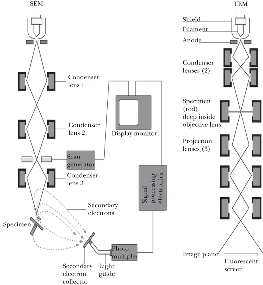
ConclusionIn summary, SEM and TEM are two important electron microscopy techniques with different operating principles, sample preparation requirements, resolution and magnification capabilities, imaging modes, and applications. SEM is used to study the surface of samples, while TEM is used to study the internal structure of samples. Both techniques have many applications in materials science, biology, physics, and other fields. They are essential tools for understanding the structure and properties of materials at the nanoscale. Choosing between SEM and TEM depends on the researcher's specific research questions and goals, as well as the nature and characteristics of the sample being studied. It is essential to note that SEM and TEM are two different techniques used for examining specimens at the micro- and nanoscale. SEM is best suited for analyzing larger, bulky samples and examining surface morphology, while TEM is best suited for analyzing thin samples and examining the internal structure of materials. SEM has a lower resolution than TEM but allows for observation at various angles and magnifications, making it a popular choice for routine analysis in industry and undergraduate laboratories. On the other hand, TEM requires more specialized equipment and sample preparation but offers high-resolution images and compositional information, making it a powerful tool for research in various fields.
Next TopicDifference between
|
 For Videos Join Our Youtube Channel: Join Now
Feedback
- Send your Feedback to [email protected]
Help Others, Please Share


