| |

Pulse Width Modulation in AVR MicrocontrollerPulse Width Modulation (PWM) is a square wave with varying low and high amplitude signal. A general PWM signal is given in a figure below: 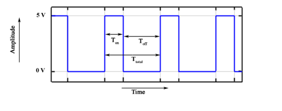
There are various terms related with the Pulse Width Modulation (PWM):
Duty Cycle:Calculation of duty cycle is done by calculating the ON-time from total period of time. It is a ratio between ON-time and total time period of the signal using period calculation, duty cycle is calculated as shown in the equation below: 
Period:As represented in the above figure, Toff represents the off-time and Ton represents the on-time of a signal. Period is a sum of both on and off times and period is calculated as shown in the equation below: 
PWM: Voltage RegulationPWM signals when operates at different duty cycle it gives a varying voltage at the output. Voltage regulation method is used in various areas of application like:
Voltage regulation operation is performed by averaging the PWM signal. Output voltage is calculated as shown in the equation below: 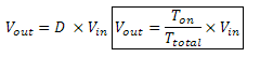
The output voltage can be directly varied by varying ON time of the pulse width modulated signal. AVR Timers as PWM:Mostly in AVR Microcontroller the on-chip PWM channel is available which makes the PWM usage much simpler and highly accurate. AVR timers and counters can be used in PWM mode of operation without disturbing the basic timer function. As in case of microcontroller (AT90S8515), Timer1 can be used in PWM mode by setting PWM10 and PWM11 bits in TCCR1A register. The following modes are available in PWM of AVR microcontroller:
The pre-scalar mode for Counter1/Timer can be selected by the use of clock select bits in TCCR1B register. Width of a pulse is loaded in a timer output compare registers OCR1A (OCR1AL & OCR1AH) and OCR1B (OCR1BL & OCR1BH). The counter1/Timer acts as an up/down counter, counting from $0000 to TOP as shown in a table below:
Here it counts and turn down again to zero before the cycle is repeated. When a counter value matches the content of 10 least significant bits of OCR1B or OCR1A, the OC1B/PD5 (OC1A) pins are cleared or set according to the settings of COM1A0/COM1A1 or COM1B1/COM1B0 bits in Timer/Counter1 control register (TCCR1A) as shown in a table below:
Note: X can be A or B register. AVR: Assembly Code for running PWM:AVR: PWM Setup in C: |
 For Videos Join Our Youtube Channel: Join Now
Feedback
- Send your Feedback to [email protected]
Help Others, Please Share


