| |

555 Timers ICThe word IC stands for Integrated Circuits. Thus, 555 timer IC is an integrated circuit chip used in various timers, pulse generators, lamp flashers, logic clocks, and oscillators. It is also known as the 555 timer oscillator. The 555 timer IC comprises various components: resistors, capacitors, RS flip-flops, comparators, BJT (Bipolar Junction Transistor), and buffers. The 555 timer IC works as a simple timer that generates pulses or produces time delays, similar to the flip-flops and oscillator. Components in the 555 Timer ICThe components of the 555 Timer IC are as follows: Resistors: The purpose of resistors in the timer is to provide voltages to the two comparators. Capacitors: It removes the voltage fluctuations in the 555 Timer IC because such fluctuations affect its operation. Transistors: BJT transistor in the timer is used as a switch. It is also used as a component that discharges the timing capacitor, which is connected externally. Flip-flops: It is an electronic circuit that changes its states from HIGH to LOW and vice-versa. Buffers: A buffer connects the input to the output, i.e., it accepts the input from the flip-flop and sends it to the output terminal. The function of the buffer is to provide adequate current to the external circuit connected to the output terminal. Comparators: It compares the voltages connected to its two input terminals (inverting and non-inverting). Pin diagram of 555 Timer ICIt is an eight-pin structure. The pin diagram of the 555 timer IC is shown below: 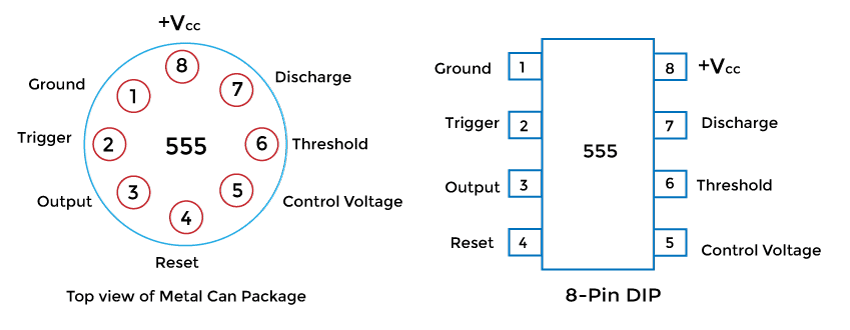
Let's discuss about each pin in detail. Pin 1: GroundThe ground terminal refers to the terminal at 0 volts and is known as a short pin. Pin 2: TriggerTrigger means activate. The trigger pin is connected to the inverting terminal in the case of the comparator (that compares two outputs). It also helps to convert the state of flip-flops from the set (1) to reset (0). The trigger pin works as a starter to the timer. It is an active low trigger that starts when the PIN 2 falls below one-third (VCC/3) of the supply voltage. Pin 3: OutputAs the name implies, it is the output of the 555 Timer IC. It means that output is available at this pin. The load can be connected between the output (PIN 3) and either to PIN 1 (output) or PIN 8 (supply). The load connected with the PIN 3 and PIN 1 is known as normally off load. It is because PIN1 is the ground pin. The load connected with the PIN 3 and PIN 8 is known as normally on load. Pin 4: ResetReset means to set again. It set the reading of the timer again to zero. We can also say that it disables the timer. To rest the 555 Timer IC, a negative pulse is applied at the PIN 4. It is not necessary to use this pin as a reset pin only. We can also connect +VCC to the reset pin to avoid any false triggering. Here, PIN 4 will not work as reset pin. Pin 5: Control voltageThe two trigger and threshold terminals at the input of the comparators are controlled using PIN 5. The output waveform of the timer can be modulated by applying an external voltage to the control voltage pin. It is connected to the ground when not in use to avoid any noise or interference in the output. Pin 6: ThresholdIt is present at the non-inverting terminal (+) of the first comparator in the 555 Timer IC circuit. It compares the applied voltage with the reference voltage (2VCC/3), connected at the inverting terminal. It determines the input state of the flip-flop. Pin 7: DischargeIt is connected internally to the collector of the BJT. A capacitor is connected between the PIN 7 and the ground, which discharges through the transistor when it reaches the saturation state. The capacitor charges when the transistor is cut-off. The external connected resistors and capacitors determine the rate of charge. Pin 8: Supply terminalAll the voltage sources are connected to this terminal. It supplies voltage to the other terminals of the IC. Functional DiagramThe functional diagram of the 55 timer IC is shown below: 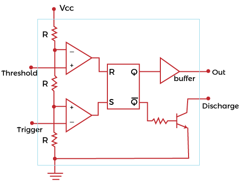
Connection Setup and operation of 555 TimerThe terminal at the top is known as VCC and the bottom terminal represents the ground. The three resistors (each labeled as R) are connected in series. Due to the potential division of the voltage with respect to the ground, the voltage at the upper comparator will be 2VCC/3, while the voltage at lower comparator is VCC/3. For the lower comparator, the (+) terminal represents the voltage VCC/3, which is compared by the voltage at the trigger input at (-) terminal of the 555 Timer. If the voltage VCC/3 is higher that the trigger input, the output of the comparator is HIGH or 1. Otherwise, it is LOW or 0. For the upper comparator, the (-) terminal represents the voltage 2VCC/3, which is compared by the voltage at the threshold input at (+) terminal of the 555 Timer. If the threshold input is higher than the 2VCC/3, the output of the comparator is HIGH or 1. Otherwise, it is LOW or 0. The comparators output is connected to the RS inputs of the flip-flops. The transition table of the RS flip-flop is shown below:
If R and S are 0, Q retains its previous state. The Q output goes into the buffer that further goes to the output of the 555 Timer. The Q' goes into the BJT switch. The output of the flip-flop Q' is opposite to the Q. If Q is 0, Q' is 1 and it turns ON the BJT. The large base current of the transistor makes it to enter in the saturation region, constituting very small current. If Q is 1, Q' is 0 and it turns OFF the BJT. The emitter end of the BJT is connected to the ground terminal and the other end is connected to the Discharge terminal of the 555 Timer. Note: BJT in the 55 Timer generally acts as a switch.Modes of the 555 Timer ICThere are three operating modes of a 555 timer IC, monostable mode, astable mode, and bistable mode. We will also discuss the working of all the three modes of the IC. Monostable ModeMonostable mode is also known as one-shot pulse generator mode. It is also called as monostable multivibrator. Diagram The internal IC circuit of the monostable multivibrator is shown below: 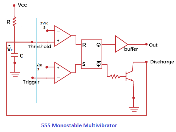
Connection setup and Working The threshold input is connection to the capacitor, which is further connected to the ground. A resistor is connected with the VCC terminal. The threshold and the discharge terminal are connected together. At the trigger input of the comparator, a negative pulse is applied, as shown below: The pulse starts from 1 goes to 0 and again reaches 1. We have assumed that the capacitor at the initial stage is uncharged. The voltage VC is 0. The output Q of the flip-flop will also be zero during the initial conditions. If trigger goes low for a short time, the output Q goes 1. The Q output remains at 1 even when the trigger goes high. The output waveform is shown below: 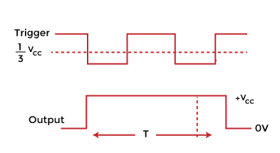
If Q = 1, Q' = 0. It means that the connection across the switch becomes the open circuit. We now have a capacitor and a resistor connected in series. The capacitor voltage (VC) starts charging or VC starts rising towards VCC. After 2VCC/3, it drops, as shown below: 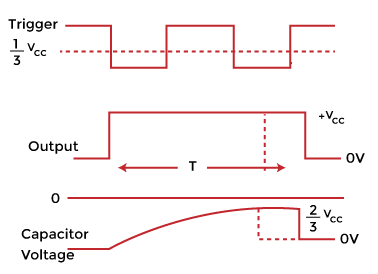
After voltage crosses 2VCC/3, the voltage at (+) of the first comparator becomes greater than 2VCC/3, where R reaches 1, S = 0, Q gets reset to 0, and Q' = 1. It closes the BJT switch, and the capacitor gets discharged through the switch. The process works at a fast rate due to the very small resistance of the switch. Hence, after 2VCC/3, Vc drops to 0. The equation of the capacitor voltage can be written as: VC(t) = VCC (1 - e-t/Y ) If t = T VC becomes equal to 2VCC/3 2VCC/3 = VCC (1 - e-T/Y ) e-T/Y = 1/3 T = Y log 3 = 1.1 Y = 1.1 RC Where, Y = tau = RC R is the capacitance of the capacitor, and R is the resistance of the resistor. T = RC log 3 Astable ModeAstable mode is also known as a free-running mode. Its output waveform is a square wave because it is an oscillator. Diagram The internal circuit diagram of the astable multivibrator is shown below: 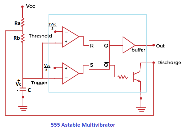
Connection setup and working The threshold input and the trigger input of both the comparators are tied together. The node between the two resistors is connected to the discharge pin. If Q is HIGH, Q' is LOW, which opens the switch and the capacitor will start charging towards the VCC. The time constant is given by: (Ra + Rb)C When the capacitor voltage reaches 2VCC/3, it drops, as shown in the below waveform. 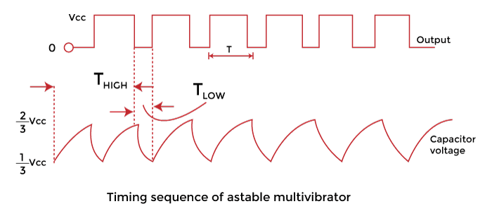
Let's discuss how. We know that S = 1 when V+ at VCC/3 is higher than 'V -,' which is the capacitor voltage. S becomes equal to 1 when VC falls below the VCC/3. Similarly, R = 1, when V+ exceeds 2VCC/3. Otherwise, R equals 0. The waveforms of the R and S with the output waveform of the oscillator are shown below: 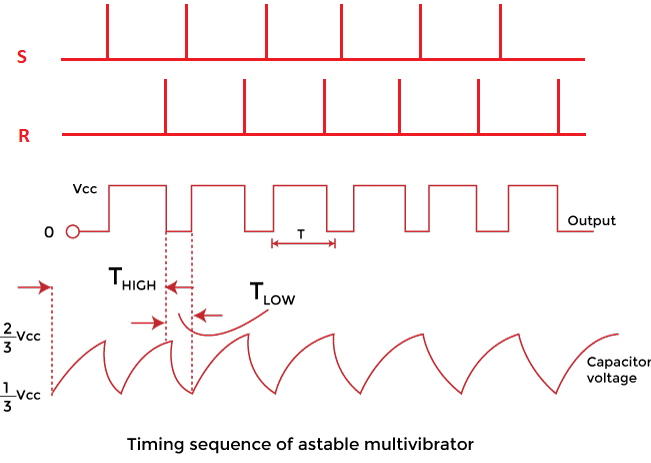
When capacitor voltage crosses 2VCC/3, R becomes 1 and S becomes 0, which resets the flip-flop to Q = 0. The Q' becomes 1 and the switch closes. The capacitor starts discharging using the path connected to the discharge pin. When VC crosses VCC/3, S becomes equal to 1, R = 0, Q = 1, Q' = 0 and capacitor starts charging towards VCC. This cycle repeats and we get the desired oscillations. During the charging state, VC (0) = VCC/3 VC (infinite) = VCC Let, VC(t) = A e-t/Y1 + B B = VCC and A = -2VCC/3 Where, Y1 = time constant = (Ra + Rb)C During the discharging state, VC (0) = 2VCC/3 VC (infinite) = 0 Let, VC(t) = 2VCC/3 e-t/Y2 If t = TL VC(t) = VCC/3 VCC/3 = 2VCC/3 e-TL/Y2 TL = Y2 log 2 With Y2 = RbC Loge2 = 0.69 So, TL = 0.69 C (Ra + Rb) Tlow = 0.69 C Rb T = 0.69 C (Ra + 2Rb) T = 1/F F = 1.45/ C (Ra + 2Rb) Bistable ModeThe 555 timers can operate in the bistable mode without the discharge pin, resistors, and capacitors. It is also known as Schmitt trigger. Features of 555 Timers ICThe features of 555 Timer IC are as follows:
Advantages of the 555 Timer ICThe advantages of the 555 timer are as follows:
Disadvantages of the 555 Timer ICThe disadvantages of the 555 timer are as follows:
Numerical ExamplesLet's discuss three examples based on the 555 Timer IC. The examples will be Multiple Choice Questions. Example 1:What is the operating mode of 555 Timer IC?
Answer: (d) Both (a) and (c) Explanation: Free-running mode: Astable vibrator mode is known as free-running mode. AS the name implies, astable does not have any stable state, but has two quasi-level states. One-shot mode: The one-shot means only one output. Thus, the 555 Timer at one-shot mode produces only one output pulse in the triggered state. Example 2:A 555 Timer IC as an astable multivibrator can be used as a:
Answer: (b) A square wave oscillator Explanation: The circuit of an astable multivibrator using the two grounded cross-coupled transistors helps it to produce the square wave output. A pair of transistors includes either an NPN or a PNP transistor with a 100% positive feedback. Example 3: What is the frequency of the astable multivibrator with the following given parameters?RA = 3.3 k Ohms RB = 5.4 k Ohms C = 0.4 uF
Answer: (c) 0.171 kHz Explanation: RA = 3.3 k Ohms = 3300 Ohms RB = 5.4 k Ohms = 5400 Ohms C = 0.4 uF = 0.6 x 10⁻⁶ Farads We know, the formula to calculate the frequency is given by: F = 1.45/ C (Ra + 2Rb) F = 1.45 / 0.6 x 10⁻⁶ (3300 + 10800) F = 1.45 x 10⁶ / 8460 F = 0.171 kHz
Next TopicClipper (electronics)
| ||||||||||||||||
 For Videos Join Our Youtube Channel: Join Now
Feedback
- Send your Feedback to [email protected]
Help Others, Please Share


