| |

Field Effect TransistorFET or Field Effect Transistor is also a type of transistor-like Bipolar Junction Transistor. FET is also known as JFET (Junction Field Effect Transistor). Let's discuss the concept, structure, types with working, and characteristics of JFET in detail. StructureThe Junction Field Effect Transistor has three terminals, drain, source, and gate. The structure and symbol of JFET are shown below: 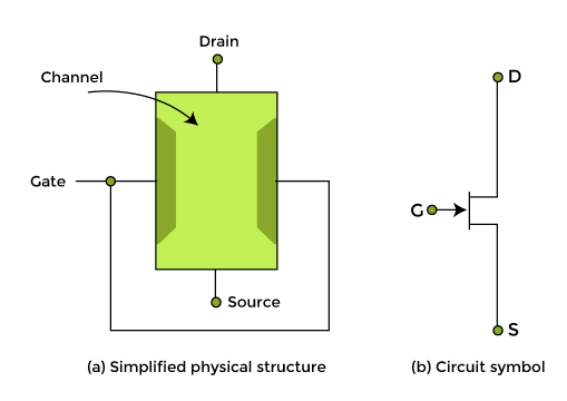
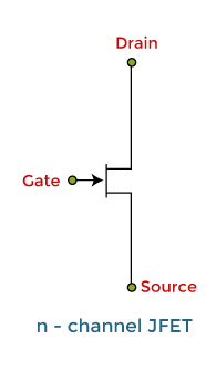
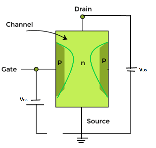
Terminals of JFETThe three terminals of JFET are as follows: SourceThe source is the terminal at the bottom of the transistor, as shown above. The majority carriers' electrons (in the case of n-channel) and holes (in the p-channel) enter through the source into the transistor. The current generated due to the majority charge carriers through this terminal is known as source current (IS). DrainA drain terminal is present at the top of the transistor. The majority carriers' electrons (in the case of n-channel) and holes (in the case of p-channel) exit from the transistor through the drain terminal. The current generated due to the majority charge carriers through this terminal is the drain current (ID). The voltage is connected across the drain and source. The direction of current in JFET is determined in the opposite direction to the flow of electrons and in the same direction to the flow of holes. The voltage between the drain and source is known as VDS. GateGate consists of the heavily doped region present on both sides of the transistor. In the case of n-channel, two p-regions are present on the two sides of the transistor, named as the gate. The same procedure creates the impurities doped on the two regions as the p-n junctions. The voltage between the gate and source is known as VGS. It is applied in the direction to make the p-n junction reverse biased. The current generated through this terminal is known as gate current (IG). ChannelThe part of the transistor where the n-type doping is present in large amounts is known as the channel. It is defined as the region between the two gate terminals that possess the movement of majority carriers from the source to the drain. VoltagesThere are two voltage sources VDS and VGS. Let's discuss the connection of these two voltage sources across the three terminals of the JFET. VDS It is the voltage across the terminals D and S, i.e., drain and source. The connection of VDS is such that its relation with the source describes the movement of charge carriers away from the S towards D. Its relation with drain describes the attraction of charge from the D to constitute the current. It can be calculated as: VDS = VD - VS VGS It is the voltage across the terminals G and S, i.e., gate and source. It is also known as the controlling voltage of JFET. It is intended to increase the drain current in the transistor. Types of JFETJFET is further categorized as n-channel JFET and p-channel JFET. The working of both the JFET are similar expect the majority carriers. N-channel JFETN-channel refers to the JFET with center channel doped with the N-type or Pentavalent impurities and the two side slabs doped with the P-type or trivalent impurities. Construction The structure of NPN JFET is shown below: 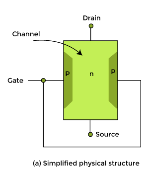
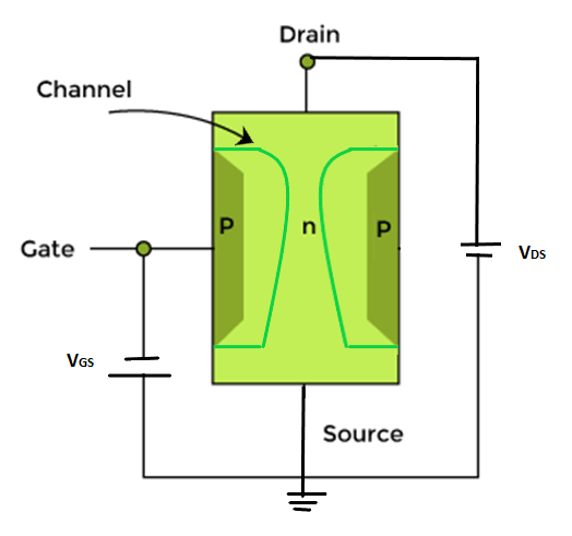
Here, D represents the Drain terminal, S represents the source, and G represents the gate terminal. VDS and VGS are the two voltage sources connected across the G, D, and S terminals. The connection is shown below: The (+) terminal of the VDS is connected to the drain and (-) terminal to the source. Similarly, the (+) terminal of the VGS is connected to the source and (-) terminal to the gate. Let's discuss its working. Working
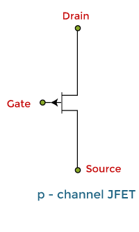
P-channel JFETP-channel refers to the JFET with center channel doped with the P-type impurities and the two side slabs doped with the N-type or Pentavalent impurities. Construction The structure of PNP JFET is shown below: 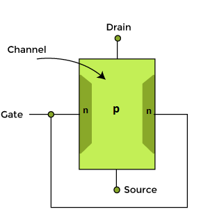
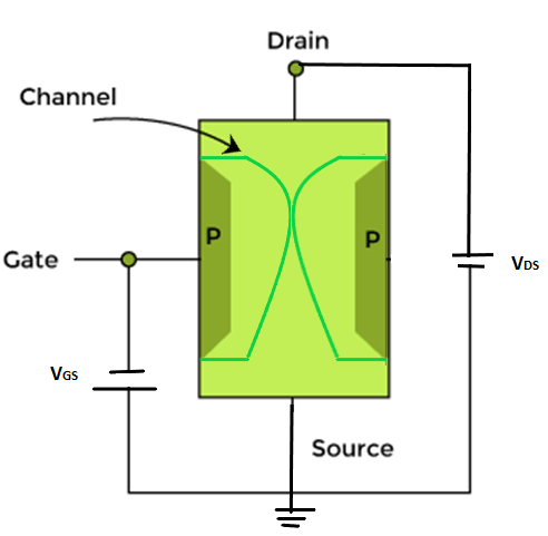
The working of the p-channel JFET is the same as that of the n-channel except for the majority charge carriers in both the Field-Effect Transistors. The charge carriers constituting the current flow in the p-channel are holes, and in the n-channel are electrons. The concept of the connection of the voltages across the three terminals is already discussed above. The depletion width in the p-channel after applying the voltage across the G, D, and S terminals will appear as: 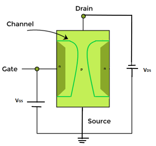
The (+) terminal of the VDS is connected to the source and (-) terminal to the drain. Similarly, the (+) terminal of the VGS is connected to the gate and (-) terminal to the source. Note: The connection of both the JFET is opposite due to the difference of majority carriers' concentration in n-channel and p-channel.JFET Formula
We will discuss two examples based on the above formula later in the topic. Pinch-off voltageIt is defined state of the transistor to turn OFF when the voltage falls below the threshold voltage VT. It is also defined as the state of the transistor that removes all the free charge from the channel. CharacteristicsHere, we will discuss the characteristics of the n-channel JFET. The characteristics with the D-S voltage on the X-axis with the drain current on the y-axis are shown below: 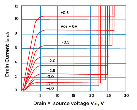
Consider the below JFET circuit. 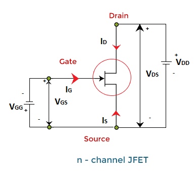
Case 1:In case of VGS = 0 and ID = 0, the S and G will not receive any voltage. It means that both terminals are open. But, when VDS is applied across the D and S terminals, the transistor will start working with the help of a small applied voltage. The electrons will move from the S towards the drain constituting the small drain current. Thus, ID will increase linearly with the applied VDS. At a point, the charge concentration will be high at the drain regions. It is a pinch-off condition, where D is more reverse biased than the S side. The current ID will start approaching the constant value. The ID responds more to VGS and slightly to VDS. Case 2:If VGS is also applied across the terminals S and D, the pinch-off condition will occur at a rapid rate as compared to the first case. It is because both the VGS and VDS are applied to the transistor. The maximum ID will also be smaller. The reverse bias voltages across the gate increase the drain voltage, increasing the effective voltage across the G junction. The n-channel JFET requires the negative voltage at the S to allow electrons to move towards the D. The D junction requires the positive voltage to attract more electrons to constitute the current. The p-channel requires positive voltage at the S to allow holes to move towards the D. The D junction requires the negative voltage to attract more holes to constitute the current. We can use either end of the channel as the source or drain, and we only need to consider the polarities applied to both channels. Mathematical modelWe have already discussed that VDS causes only a small change in the drain current of the transistor. But when VGS is applied, the current increases. Let's consider the effective channel cross-section be A, which is constant. Area of A = 2bw Where, 2b is the channel width W is the channel dimension perpendicular to the width The drain current based on the Ohm's law can be written as: ID = AqNDunε Putting the value of A = 2bw, we get: ID = 2bwqNDunε Where, ND is the donor ions We know ε = VDS/ L So, ID = 2bwqNDunVDS/ L FET as a Voltage Variable ResistorFET can work as a VVR in a specific region, and voltage Variable Resistor is also known as Voltage Dependent Resistor. The Field Effect transistor constitutes a small drain current when VDS is small, and it is the state before the pinch-off. The transistors work like a Voltage Variable Resistor in this region only, i.e., before the pinch-off. The resistance across the two junctions, D and S, is controlled by the voltage VGS. The VVR is used in various applications, such as audio amplifiers and television receivers. FET vs. BJTLet's discuss the differences between the Field Effect Transistor and Bipolar Junction Transistor.
Numerical ExamplesLet's discuss two examples of JFET. Example 1: A Junction Field Effect Transistor produces a gate current of 5nA. The gate is reverse biased at the voltage of 10 volts. Find the resistance between the drain and source terminal of the transistor? Solution: Given: VGS = 10V and IG = 5nA We need to find the RGS We know, RGS = VGS / IG Putting the values in the given formula, we get: RGS = 10 / 5 x 10⁻⁹ RGS = 2 x 10⁹ Ohms RGS = 2000 x 106 Ohms Or RGS = 2000 Mega Ohms Example 2: Find the drain current with the following parameters: IDSS = 5mA VGS = -2 Volts VP = -1 volts Solution: We know the formula to find the drain current is given by: ID = IDSS (1 - VGS/VP)2 Putting the given values in the above equation, we get: ID = 5 x 10⁻³ (1 - (-2 /-1))2 ID = 5 x 10⁻³ (1 - (2))2 ID = 5 x 10⁻³ (-1)2 ID = 5 x 10⁻³ Amperes Or ID = 5mA Thus, we can say that ID = IDSS = 5mA Example 3: Find the pinch-off voltage of the n-channel silicon JFET with the following parameters: ND = 1016 cm-3 A = 0.40um ε = 8.854 x 10⁻¹⁴ Solution: We know, the formula to calculate pinch-off voltage is given by: VP = qNDa2/2εs εs = ε εo q is the charge of an electron = 1.6 x 10⁻¹⁹ Putting the given values in the above equation, we get: VP =1.6 x 10-19 x 1016 x (0.4 x 10-4)2 /2 x 11.7 x 8.854 x 10-14 VP = 1.23 Volts
Next TopicSmallest odd number
|
 For Videos Join Our Youtube Channel: Join Now
Feedback
- Send your Feedback to [email protected]
Help Others, Please Share


