| |

What is PCB?A Printed circuit board (PCB) is the foundational building block of electronic devices. PCB is the foundation on which all of the other electronic components are assembled onto. It mechanically supports and electrically connects electronic components using conductive tracks, pads, and other features etched from one or more sheet layers of copper laminated onto and between sheet layers of a non-conductive substrate. Components are generally soldered onto the PCB to both electrically connect and mechanically fasten them to it. They are also used in some electrical products, such as passive switch boxes. PCBs require additional design effort to lay out the circuit, but manufacturing and assembly are automated. Electronic computer-aided design software is available to do much of the work of layout. Mass-producing circuits with PCBs are cheaper and faster than with other wiring methods. Large numbers of PCBs can be fabricated simultaneously, and the layout only has to be done once. PCBs can also be made manually in small quantities. PCBs can be single-sided, double-sided, or multilayer. Multi-layer PCBs allow for much higher component density because circuit traces on the inner layers would take up surface space between components. The rise in popularity of multilayer PCBs with more than two, and especially with more than four, copper planes was concurrent with the adoption of surface mount technology. However, multilayer PCBs make repair, analysis, and field modification of circuits much more difficult and usually impractical. The world market for bare PCBs exceeded $60.2 billion in 2014 and is estimated to reach $79 billion by 2024. Structure of PCBThe structure is the arrangement of conductive and insulating layers in a multilayer PCB. There are alternating layers of different materials which are laminated together with heat and adhesive. The following image shows the structure of a four-layer board. 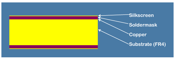
1. Substrate The base material or substrate is usually fiberglass. The most common designator for this fiberglass is FR4. This solid core gives the PCB its rigidity and thickness. There are also flexible PCBs built on flexible high-temperature plastic. You will find different thickness PCBs. The most common thickness for SparkFun products is 1.6mm. Some of our products, such as LilyPad and Arduino Pro Micro boards, use a 0.8mm thick board. Cheaper PCBs and perf boards will be made with other materials such as epoxies or phenolics, which lack the durability of FR4 but are much less expensive. 2. Copper The next layer is a thin copper foil, which is laminated to the board with heat and adhesive. In lower-cost electronic gadgets, the PCB may have copper on only one side. When we refer to a double-sided, we refer to copper as applied to both sides of the substrate. This can be as few as 1 layer or as many as 16 layers or more. The copper thickness can vary and is specified by weight, in ounces per square foot. The vast majority of PCBs have 1 ounce of copper per square foot, but some PCBs that handle very high power may use 2 or 3-ounce copper. Each ounce per square translates to about 35 micrometers or 1.4 thousandths of an inch of thickness of copper. 3. Soldermask The layer on top of the copper foil is called the solder mask layer. This layer gives the PCB its green. It is overlaid onto the copper layer to insulate the copper traces from accidental contact with other metal, solder, or conductive bits. This layer helps the user to solder to the correct places and prevent solder jumpers. Soldermask is most commonly green in color, but nearly any color is possible. We use red for almost all the SparkFun boards, white for the IOIO board, and purple for the LilyPad boards. 4. Silkscreen The white silkscreen layer is applied on top of the solder mask layer. The silkscreen adds letters, numbers, and symbols to the PCB that allow for easier assembly and indicators for humans to understand the board. We often use silkscreen labels to indicate the function of each pin or LED. Silkscreen is most commonly white and widely available in any ink color such as Black, gray, red, and yellow. Terminology of PCBHere are some terminologies which used in PCB structure, such as:
Types of PCBThere are several different types of printed circuit boards, each with its particular manufacturing specifications, material types, and usages: 1. Single-layer PCB A single-layer or single-sided PCB is made out of a single layer of base material or substrate. One side of the base material is coated with a thin layer of metal. Copper is the most common coating due to how well it functions as an electrical conductor. Once the copper base plating is applied, a protective solder mask is usually applied, followed by the last silkscreen to mark all of the board's elements. 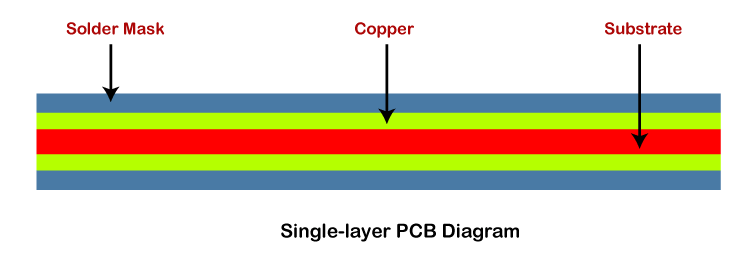
Since single-layer PCBs only have their various circuits and components soldered onto one side, they are easy to design and manufacture. They can be purchased at a low cost, especially for high-volume orders. They are commonly used for various applications, including calculators, cameras, radio, stereo equipment, solid-state drives, printers, and power supplies. 2. Double-layer PCB Double-layer or double-sided PCBs have a base material with a thin layer of conductive metal, like copper, applied to both sides of the board. Holes drilled through the board allow circuits on one side of the board to connect to circuits on the other. 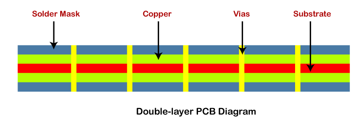
The circuits and components of a double-layer PCB board are usually connected in one of two ways: either utilizing a through-hole or using a surface mount. Double-sided PCBs are typically used in applications that require an intermediate level of circuit complexity, such as industrial controls, power supplies, instrumentation, HVAC systems, LED lighting, automotive dashboards, amplifiers, and vending machines. 3. Multi-layer PCB Multi-layer PCBs consist of a series of three or more double-layered PCBs. These boards are then secured together with specialized glue and sandwiched between pieces of insulation to ensure that excess heat doesn't melt any of the components. 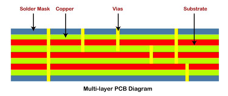
Multi-layer PCBs come in various sizes, going as small as four or as large as ten or twelve layers. The largest multilayer PCB ever built was 50 layers thick. With many layers of PCBs, designers can make very thick, complex designs suitable for a broad range of complicated electrical tasks. Applications where multilayer PCBs would be beneficial include File servers, Data storage, GPS technology, Satellite systems, Weather analysis, and Medical equipment. 4. Rigid PCB Rigid PCBs are made out of a solid substrate material that prevents the board from twisting. The most common example of a rigid PCB is a computer motherboard. Rigid PCBs make up perhaps the largest number of PCBs manufactured. Rigid PCB can be used in any position where the PCB itself needs to be set to a shape and maintained during the remaining life of the equipment. All Rigid PCBs have single-layer, double-layer, or multilayer constructions, so they all share the same applications. 5. Flexible PCB Unlike rigid PCBs, which use unmoving materials such as fiberglass, flexible printed circuit boards are made of materials that can flex and move, such as plastic. Like rigid PCBs, flexible PCBs come in single, double, or multilayer formats. As they need to be printed on a flexible material, flexible PCB cost more for fabrication. 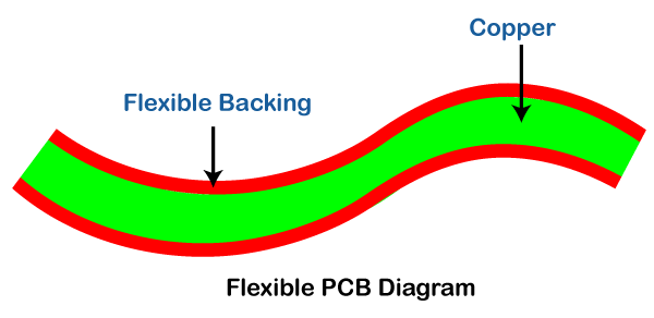
Flexible PCBs offer many advantages over rigid PCBs. They can be folded over edges and wrapped around corners. Their flexibility can lead to cost and weight savings since a single flexible PCB can cover areas that might take multiple rigid PCBs. 6. Rigid-Flex PCB Rigid-flex boards consist of multiple layers of flexible PCBs attached to many rigid PCB layers. 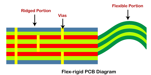
Flex-rigid PCBs have a lower parts count than traditional rigid or flexible boards because the wiring options for both can combine into a single board. Combining rigid and flexible boards into a single rigid-flex board also allows for a more streamlined design, reducing the overall board size and package weight. Flex-rigid PCBs are most often found in applications where space or weight are prime concerns, including Cell phones, Digital cameras, Pacemakers, and Automobiles. 7. High-frequency PCB High-frequency PCB refers to a general PCB design element rather than a PCB construction like the previous models. High-frequency PCB is designed to transmit signals over one gigahertz. High-frequency PCB materials often include FR4-grade glass-reinforced epoxy laminate, polyphenylene oxide (PPO) resin, and Teflon. Teflon is one of the most expensive options available because of its small and stable dielectric constant, small amounts of dielectric loss, and overall low water absorption. 8. Aluminum-Backed PCB Aluminum-backed PCBs are designed in much the same way as their copper-backed counterparts. However, instead of the usual fiberglass used in most PCB board types, aluminum circuit board uses aluminum or copper substrate board. 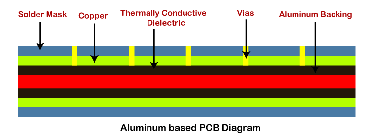
The aluminum backing is lined with thermally insulating material designed to have a low thermal resistance, which means less heat is transferred from the insulating material to the backing. Once the insulation is applied, a circuit layer of copper ranging in thickness from one ounce to ten is applied.
Next TopicProgram to Convert Feet to m
|
 For Videos Join Our Youtube Channel: Join Now
Feedback
- Send your Feedback to [email protected]
Help Others, Please Share


