| |

DiodeA diode is an electronic device that conducts current in only one direction under specific voltage. It is a two-terminal device, which depicts the positive and negative terminal. An ideal diode has zero resistance in a particular direction. We can also say that it has high resistance in the other direction. Here, infinite resistance means zero current flow through the circuit. Hence, we can say that an ideal diode conducts current in one only direction due to infinite resistance or zero current in other direction. In the case of real diodes, infinite resistance does not exist. We can say it as high resistance. Here, we will discuss the effect of forward and reverse bias on the diode and various types of the diode. But, from the diodes list, the Zener diode is the only diode that can conduct current in both forward and backward directions. We will discuss Zener diodes later in the topic. Effect of Bias on the DiodeThe bias signifies the forward and reverse bias in the diode. Let's discuss this in detail.
Types of DiodesThere are various types of diodes with different uses. The diodes are mainly categorized as vacuum diodes, signal diode, and semiconductor diodes. Let's discuss the types of a diode in detail. Here, we will also discuss their applications. Vacuum diodeVacuum diodes are considered the simplest production to control the free electrons. The two electrodes of the vacuum diode are cathode and anode. A filament in the diode heats the cathode element. The uses of such diodes were reduced after the invention of semiconductor diodes. But, vacuum diodes are still used today in few high-power applications. It is due to the robustness and voltage tolerance ability over other semiconductor diodes. Applications The applications of vacuum diodes are listed below:
Signal diodesThe signal diodes are further categorized as:
Let's discuss a short description of the two types of the signal diode. Small signal diodeThe small-signal diodes come with low current and power ratings. It can perform better for the high-frequency applications. The pulse amplitude of such diodes ranges to few volts. Large signal diodeThe p-n junction of the large signal diode is large. But, it is not suitable for high-frequency applications like small-signal diodes. Applications The common applications of small signal diodes are listed below:
The common application of the large signal diode is as follows:
Semiconductor diodesSemiconductor diodes are the common type of diodes. It was the first to develop among semiconductor devices. The different types of semiconductor diodes are listed below:
Junction diodesHere, we will discuss the common types of junction diodes. Junction diodes are characterized as:
Let's discuss the above type of junction diodes in detail. P-N Junction Diodes The combination of the p and n side results in the p-n junction diode. The electron flows from the n-side to the p-side contributing to the flow of current in the circuit. The impurities are added on the p-side and n-side to increase the charge carriers' concentration in the diode. The n-side comprises of majority carriers electrons and positively charged ions known as donors. The p-side comprises of majority carriers holes and negatively charged acceptor ions known as immobile ions. The p-n junction diode is shown below: 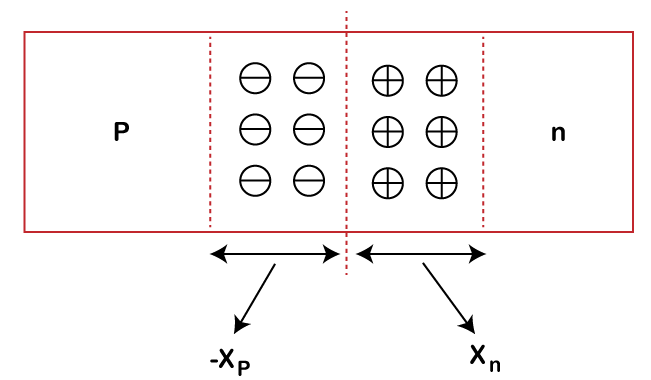
Here, Xp and Xn are the charged ions. If one side of the p-n junction is highly doped compared to the other, the diode is known as the abrupt p-n junction diode. An abrupt p-n junction (either heavily doped on one side or both sides) offers dynamical resistance for a longer range of applied potential difference. Applications The applications of p-n junction diodes are listed below:
Varactor DiodesThe varactor diode is a p-n junction diode used for varying capacitance across the junction. The depletion region of a p-n junction diode containing donors and acceptors ions plays a role like a variable capacitor under biasing. The varactor diodes are used in tuning circuits. It also provides usable dc voltage to tune a circuit, for example, simple remote control or automatic tuning function device. Applications The application of Varactor diode is as follows:
Zener DiodesZener diode is the heavily doped p-n junction diode. The p-n junction of the Zener diode is heavily doped to get a narrow depletion region. The narrow depletion region allows the ions to gain energy from the external source quickly. In the reverse bias, the junction potential of the Zener diode is increased. It results in an increased current through the Zener diode. The symbol of the Zener diode is shown below: 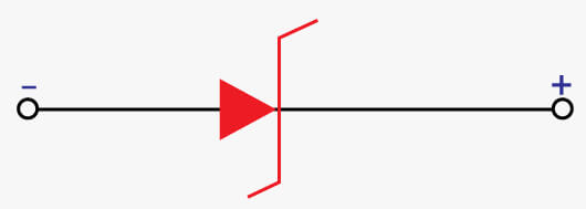
The Zener diode's advantages include voltage protection, low cost, voltage shift, better performance, and operation at high voltages. Hence, the Zener diode is preferred for applications, such as waveform clippers, voltage regulators, etc. The structure of the circuit comprising of the Zener diode is shown below: 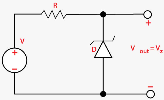
The resistor in series is connected with the diode to limit the excess current that may damage the diode. Applications The applications of the Zener diode are listed below:
Switching DiodesA p-n junction diode can be used as a switch between conducting and non-conducting state if the depletion region's space charge is controlled along with the carrier lifetime. The switching characteristics of a p-n junction diode should store a small charge. It should have a short carrier lifetime for the hole. When the switching diode operators in the reverse bias conduction, little time is required to remove the neutral region's stored charge. Applications The application of switching diodes is as follows:
Schottky DiodesThe working concepts of Schottky diodes are different from the ordinary p-n junction diodes. The difference lies in the rectification that occurs due to the difference in the work function values of metal and semiconductor. The other differences between the Schottky diodes and ordinary p-n junction diodes are non-uniform doping and conduction controlled by majority carriers' saturated emissions. It means that the recombination of minority carriers cannot govern the switching speed of the Schottky diode. Thus, the switching rate is a majority carrier phenomenon. The common advantages of the Schottky diode include less noise, better performance, and fast recovery time. Applications The applications of Schottky diodes are listed below:
Optoelectronic diode devicesThe optoelectronic devices are the devices based on the interaction between photon and materials. There are three possible ways in which a photon can interact with the material and undergo absorption, spontaneous emissions and stimulated emissions. The energy of the incident photon in such diodes should be greater than the bandgap energy to excite an electron from the valence and to the conduction band. The optoelectronic diode devices are characterized as:
Let's discuss the above types of diodes in detail. P-n junction PhotodiodeA p-n junction photodiode is an ordinary photodiode. The reverse saturation current in the photodiode flows due to the minority carriers in the reverse bias. The depletion width in the case of reverse bias is large. A photon with energy higher than the bandgap energy is absorbed in the material. It transfers some of its energy to other electrons present in the upper part of the valence band. Such electrons that receive energy are excited to the conduction band. Hence, an electron-hole pair is generated in the depletion region. The applied depletion field separates these electron-hole pairs to execute the reverse current. Hence, the magnitude of the produced photocurrent depends on the responsivity and quantum efficiency. The circuit of the p-n junction photodiode is shown below: 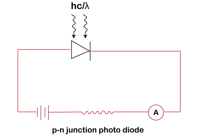
Applications The applications of p-n junction photodiode are listed below:
P-i-n junction PhotodiodeThe lightly doped layer of intrinsic material is sandwiched between the heavily doped p and n layers. The combination of the three layers results in the increase of depletion region width. The enlarged depletion width is utilized for the incidence of the photons. The photo carriers generated in the depletion width are collected much faster by the net bias voltage across the region. The collection process is much faster than the diffusion process. The circuit of the p-i-n junction photodiode is shown below: 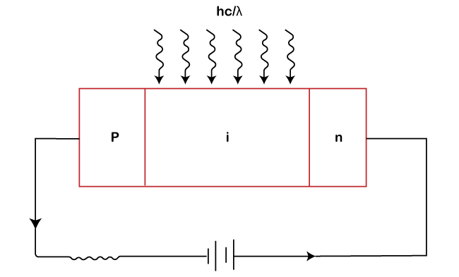
The excitation of the electrons results in the creation of electron-hole pair. The high electric field separates the generated electron-hole pair in the depletion region due to reverse bias. It further gives rise to the flow of current known as photocurrent. Applications The applications of the p-i-n junction photodiode are listed below:
Avalanche PhotodiodesThe avalanche photodiode is used in the detection of low-intensity optical signals. It is due to the impact ionization process, which is also responsible for avalanche breakdown. The circuit of avalanche photodiode is shown below: 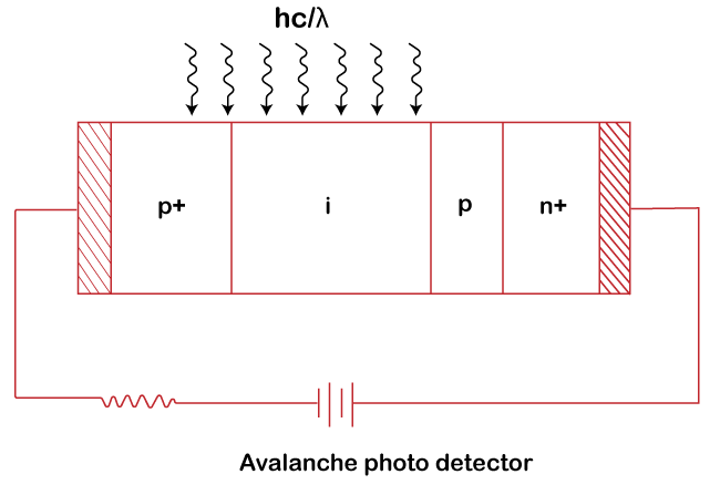
It comprises the lightly doped p-slab and the combination of intrinsic semiconductor layers sandwiched between the heavily doped p and n layers. Such combination in an avalanche diode provides extra length to the depletion region of the diode. It further results in an increased number of atoms and acceptors. A large number of charge carriers is present at the boundary of the depletion region. Applications The applications of avalanche photodiodes are listed below:
Light Emitting DiodesThe LED or Light Emitting Diodes are a p-n junction diode with an energy gap in the range required for visible light production. The forward voltage applied to the p-n junction diode allows the majority carriers to move quickly between the neutral regions. The electromagnetic radiation produced in the diodes is like a particle occupying a high energy state to low energy. It is due to the recombination of a majority carrier electron with the majority carrier hole. The LED symbol is shown below: 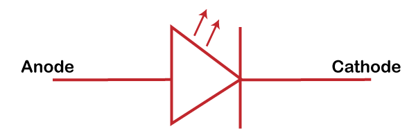
The structure of Light Emitting diode is shown below: 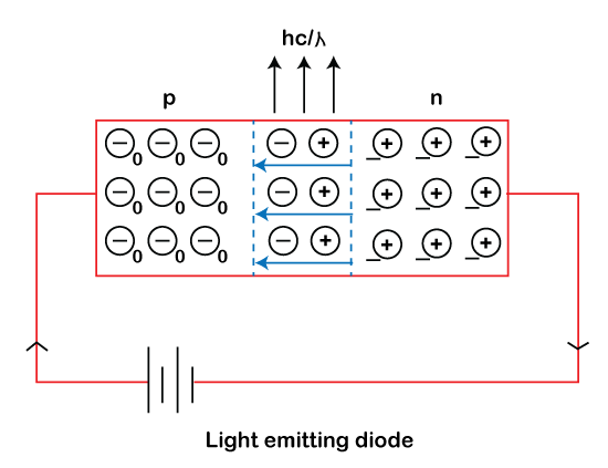
Applications Some of the common applications of the Light Emitting Diodes are listed below:
Gunn DiodeThe Gunn diode is an n-type GaAs (Gallium Arsenic) diode. It works with different conduction band energy levels. The transfer of electrons occurs from the lower conduction band energy level to the higher conduction band energy level. The transferred electron at the conduction band's upper energy level is free than the electron at the lower energy level. Applications The applications of Gunn diode are listed below:
Laser diodesAn optical cavity or a resonant cavity comprising of the LED with parallel polishes faces is known as lasers. Such diodes are generally preferred for barcode readers, optical communications, laser scanning, etc. It is also known as an injection laser diode. The laser diodes are responsible for converting the electrical energy in the form of light. Applications Some of the common applications of the laser diodes are listed below:
Impatt diodesIMPATT or Impact Ionization Avalanche Transit Time Diode is the n-p-i-p junction diode. The structure of the IMPATT diode is shown below: 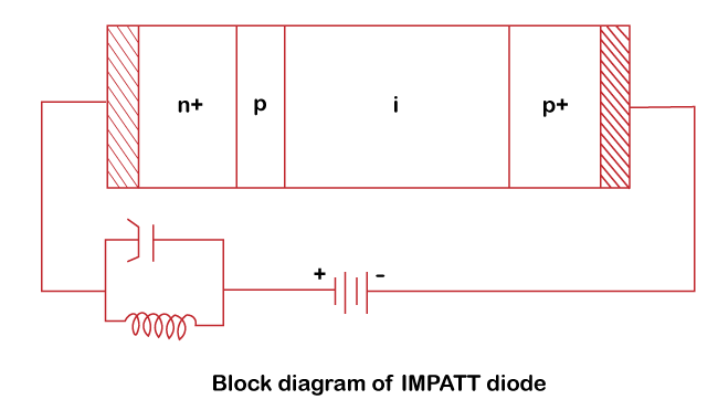
The two corner p and n layers of the diode are heavily doped. It signifies the intrinsic layer in the diode. The mechanism of the devices is based on two regions:
The lightly doped p-region is present at the boundary where avalanche multiplication takes place. Such a region is also called an avalanche region or high field region. The i-region is the intrinsic region, which is also known as the drift region. The depletion region obtained between the n-p and i-p layer is called a space-charge region. Applications The applications of Impatt diode are listed below:
PIN diodesThe PIN diode signifies a diode with a combination of a semiconductor layer of p-type, intrinsic, and n-type. The intrinsic semiconductor layer between the p and n-type is the undoped (no doping present) layer. In comparison, the other two semiconductor layers are highly doped (p-type and n-type). The reason for the two reasons being heavily doped is for the ohmic contacts, which are considered a non-rectifying electrical junction. Applications The applications of the PIN diodes are listed below:
Note: The PIN diodes are different from the p-i-n photodiodes. The role of PIN diodes is limited. While the functions of p-i-n photodiodes are low sensitivity, high-intensity electric field region, etc.
|
 For Videos Join Our Youtube Channel: Join Now
Feedback
- Send your Feedback to [email protected]
Help Others, Please Share


