| |

Zener diodeWhen a heavily doped p-n junction diode improves to work in the reverse breakdown region, it is known as Zener diode. The fabrication of the Zener diode is created such that it can easily operate in the reverse breakdown region. The symbol of the Zener diode is shown below: 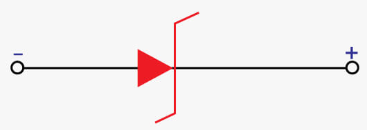
The Zener diode's advantage is that it continues to operate in the reverse bias mode without getting damaged. The Zener diode is used in various applications, such as voltage regulators, voltage shifter, voltage stabilizers, etc. Let's first discuss the common terms required to better understand the Zener diode concept and its reverse breakdown process. DopedDoping refers to the process of adding impurities to a substance or material. The motive of adding impurities is to increase the electrical and structural properties of a substance. Heavily dopedA substance with a high concentration of impurities is known as a heavily doped substance. It increases the number of charge carriers, which further increases the conductivity of a material. Reverse biasA reverse bias allows very little current to flow through the diode, while a forward bias allows a large current to flow through it. The reverse bias mechanism in the Zener diode is not destructive. The excessive heat generated by the flow of large reverse current and voltage fluctuations may cause a diode in no-use condition. Why is reverse bias preferred over forward bias?The forward current in a Zener diode easily allows the flow of current in the diode. The graph in such a case is generally exponential. The excessive current may damage the junction of the diode due to heating. Hence, a forward bias is not preferred for the breakdown mechanism in the Zener diode. Why is the p-n junction of the zener diode heavily doped?The p-n junction of the Zener diode is heavily doped to get a narrow depletion region. The narrow depletion region allows the ions to easily gain energy from the external source. In the reverse bias, the junction potential of the Zener diode is increased. It results in an increased current through the Zener diode. Let's discuss it in detail. The Zener voltage value is an essential factor. The increase in junction temperature results in the decrease of Zener voltage value, which is the basic requirement for the diode's better functioning in reverse bias. We can control it by adjusting the thickness of the depletion region. Thus, to maintain the thickness of the depletion region, the diode is heavily doped. It means that a heavily doped region can behave like a Zener breakdown region, while a lightly doped p-n junction cannot. Now, let's first discuss the p-n junction concept and the effect of reverse bias on the p-n junction. P-N JunctionWhen the p-n junction is connected to the external voltage, it is said to be under biasing. The biasing on the p-n junction can be forward bias or reverse bias. When the battery's positive terminal and the negative terminal is connected to the p side and the n-side of a battery, the junction is said to be in forward bias. Similarly, when the battery's positive terminal and the negative terminal is now connected to the n and p side, the junction is said to be in reverse bias. Let's discuss the reverse bias condition of the p-n junction in detail. Reverse bias condition in a p-n junctionWhen a negative voltage is applied to the p-type semiconductor, the valence band's potential energy in the junction gains energy. The increase in potential energy gives rise to the valence band edge, as shown below: 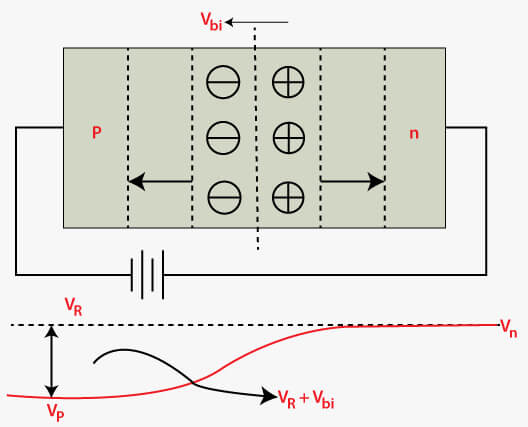
The above diagram depicts the split of Fermi energy level and bends downwards, going from the p-region to the n-region. Due to the rise of the valence band edge, the electrons on the n-side and holes on the p-side find increased width potential energy barrier, as shown below: 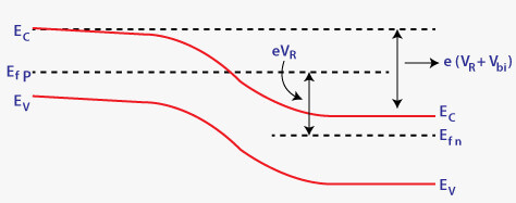
Hence, the majority carries in the junction do not saturate at terminals moving opposite to each other and do not contribute to the recombination current. The minority carriers holes and electrons are the only carriers that gain energy and execute recombination current known as reverse saturation current. A p-n junction diode offers high resistance in the reverse current due to collisions near the junction. Under reverse bias, the drift current is reduced in comparison to the diffusion current. Zener diodeThe applied electric field in the Zener diode is large, and the depletion region's width is very small. The same happens for a small bias voltage of 5V. The large electric field and depletion width allow the electrons to tunnel from the valence band of the p-type of the heavily doped p-n junction to the conduction band of the n-type. A conventional diode under the application of reverse bias can permanently damage the diode. The Zener diode's characteristics are similar to other diodes but are specially designed with reduced breakdown voltage. Such voltage is termed as Zener voltage. The current across the Zener diode remains close to the Zener voltage. Hence, it is used in different applications, such as voltage regulation, voltage stabilizers, etc. OperationThe structure of a zener diode is shown below: 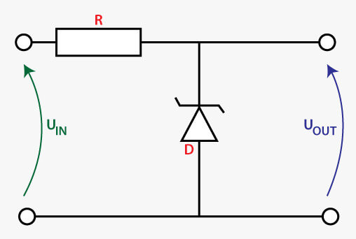
The above diagram depicts the connection of the p-n junction under reverse bias. It is a simple p-n junction diode but heavily doped. It means extra impurities are added to the semiconductor. The V-I characteristics of a Zener diode are shown below: 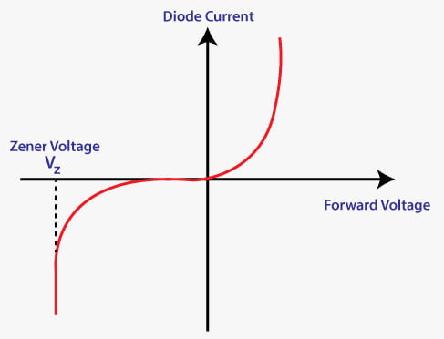
The diode operating in forward biased acts as a simple diode. In the case of reverse bias, the The increase in reverse bias increases the current flow through the diode. The resistor connected in series to the diode maintains the current and prevents the diode from damaging. As soon as the voltage in the circuit reaches the maximum value, the limiting resistor stabilizes the voltage level and makes it constant for a certain duration. When the voltage reaches the reduced breakdown voltage or Zener voltage, the electric field becomes strong. The produced electric field is strong enough to excite electrons from the valence band. A small increase in the voltage of the Zener diode results in a rapid spike in the current. Let's discuss the breakdown mechanism in the Zener diode in detail. Zener breakdownBreakdown in the p-n junction is the rapid increase in the flow of current under the reverse bias. Such voltage is known as the breakdown voltage. Zener breakdown mechanism depends on the doping. It means the higher doping will decrease the breakdown voltage of the zener diode. The zener diode has a small depletion width. The minority charge carriers in the heavily doped p-n junctions can easily tunnel through the depletion region due to its high depletion electric field. The tunneling provides acceleration to the minority carriers. These carriers collide with the available donor and acceptor ions near the junction to generate more electron-hole pairs. The generation of such a large electron-hole pair increases the reverse saturation current, known as zener breakdown. We know that the electron jumps from the valence band to the conduction band. Similarly, in this reverse mechanism, the electrons tunnel through the barrier from the filled valence band states of the p-region to the unfilled states in the n-region. Hence, the junction in such a case is not damaged. It comes back to its original state after the removal of reverse bias. Characteristics of Zener diode
Applications of Zener diodeLet's discuss some common applications of the Zener diode. 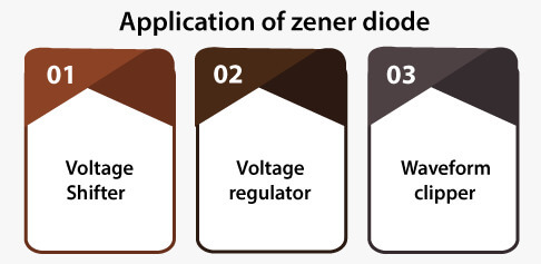
Voltage ShifterThe Zener diodes are the diode that can allow the current to flow anode to cathode and vice-versa. The voltage shifting capability of the circuit allows compatibility between various voltage requirements. The connection of the voltage shifter is such that the anode (positive terminal of Zener diode) is connected to the output, while the cathode terminal is connected to the source with the pull-down resistor. Voltage RegulatorThe Zener diode operates in the reverse bias. The use of a Zener diode in the voltage regulator provides a constant output voltage instead of different voltage fluctuations. It saves the devices from damage in high voltages. Let's discuss the use of the Zener diode in the voltage regulator in detail. The circuit of the voltage regulator is shown below: 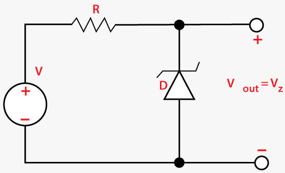
The resistor in series is connected with the diode to prevent it from excessive current. Such a resistor is also known as a limiting resistor. Waveform clipperIn the waveform clipper circuit, the Zener diode acts as a biasing diode, where the biasing voltage in the circuit is equal to the breakdown voltage. Let's discuss the role of Zener diode in waveform clipper. The waveform clipper comprises a resistor in series with the Zener diode. The resistor prevents the diode from excessive current. There are two diodes arranged upside down, as shown above. The diodes are arranged such that it provides clipping Zener voltage at both positive and negative input cycles. To obtain a single output cycle (positive or negative), we can use a single Zener diode in the circuit. 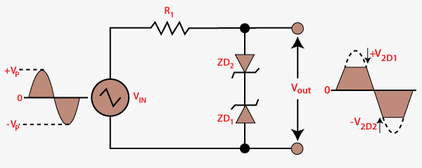
The input cycle comprises of positive half and negative half. During the positive half of the cycle, one diode is reversed biased, and the other is forward biased. Similarly, it happens during the negative half cycle. In such a case, the output waveform is clipped as the addition of Zener voltage and forward voltage of 0.7V. Advantages of zener diodeZener diode allows the current to flow in both forward and backward directions. In the case of other diodes, the current can flow in only one direction. The advantages of Zener diode are listed below:
Disadvantages of Zener diodeThe disadvantages of the Zener diode are listed below:
Avalanche BreakdownW e have already discussed about zener diode. Let's discuss the avalanche breakdown. Avalanche breakdown is caused by the impact ionization of acceptor and donor ions in the depletion region. It is primarily observed in lightly doped p-n junctions. The depletion width is large. The process of generating electron-hole pairs due to the collision of minority carriers with the donors and acceptors is known as impact ionization. These electron-hole pairs are created almost in the middle part of the depletion region. The high electric field quickly separates the generated electron-hole pairs. It further collides with more charges ions, which results in more number of electrons and holes produced. It further causes a large reverse saturation current. This stage of increasing reverse bias where a sharp rise in reverse current occurs is known as avalanche breakdown. Zener Breakdown vs. Avalanche breakdownThere are two breakdown mechanisms called avalanche breakdown and Zener breakdown. But, both of these breakdown mechanisms are not destructive. The difference between these mechanisms is the breakdown under reverse bias depending upon minority carriers available inside and outside the depletion region. Let's now discuss the difference between these two mechanisms for better understanding.
The difference in the VI characteristics of the Zener and avalanche breakdown is shown in the below image: 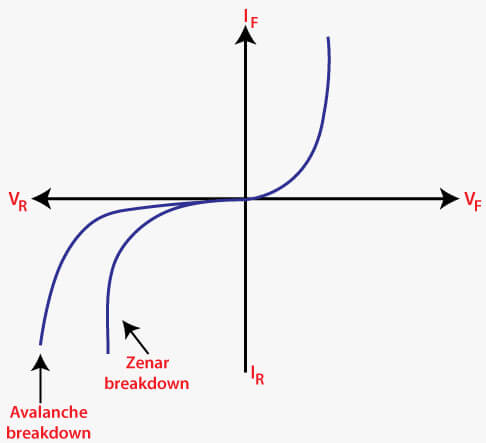
It clearly depicts that the curve of the Zener breakdown is sharper as compared to the avalanche breakdown.
Next TopicTop 10 Beer brands in India
|
 For Videos Join Our Youtube Channel: Join Now
Feedback
- Send your Feedback to [email protected]
Help Others, Please Share


