| |

CMOSCMOS or Complementary Metal Oxide Semiconductor is a combination of NMOS and PMOS transistors that operates under the applied electrical field. The structure of CMOS was initially developed for high density and low power logic gates. The NMOS and PMOS are the types of Metal Oxide Semiconductor Field Effect Transistors (MOSFET). The CMOS transistors are used in various applications, such as amplifiers, switching circuits, logic circuits, Integrated circuit chips, microprocessors, etc. The importance of CMOS in semiconductor technology is its low power dissipation and low operating currents. Its manufacturing requires fewer steps as compared to the Bipolar Junction transistors. As discussed, CMOS is a combination of NMOS and PMOS transistors. Let's discuss a short description of the NMOS and PMOS transistor before beginning with CMOS. NMOSThe symbol of the NMOS transistor is shown below: 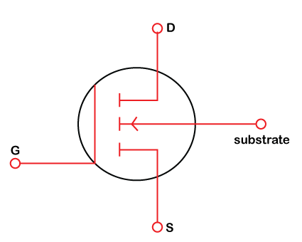
The n-channel MOSFET is called NMOS. It has a substrate of p-type, which consists of majority carriers holes. The n-channel consists of majority carriers electrons. The flow of electrons is fast as compared to holes. Hence, NMOS transistors are more rapid than PMOS transistors. PMOSThe symbol of the PMOS transistor is shown below: 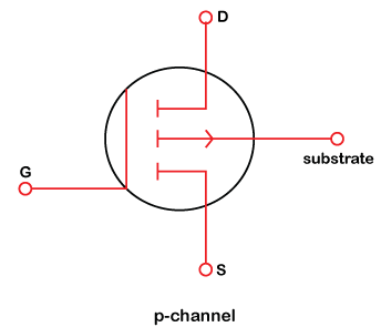
The p-channel MOSFET is called PMOS. It has a substrate of n-type, which consists of majority carriers electrons. When a negative voltage is applied to the gate end of the PMOS, it repels the electrons. The attraction of holes results in the formation of the channel called the p-channel. The channel is formed between the source and drain. The slow flow of holes makes the current controlled process of PMOS easy as compared to NMOS transistors. Connection setup of CMOSThe practical construction of the CMOS transistor is shown in the below image: It comprises the NMOS transistor that has N++ regions at the source and drain terminal and p-type substrate. Similarly, the PMOS transistor has two P++ regions and an n-type substrate. Working of CMOSThe structure as shown consists of the NMOS transistor inverted on the top of the PMOS transistor. The substrate is of the P-type, and three N++ regions. The two N++ regions are small and the third N++ region is large. The two smaller regions are a part of the NMOS transistor, while the third N++ region is a part of the PMOS transistor. The two P++ regions are diffused into the larger N++ region to form the PMOS transistor. The top surface is protected and covered using the Silicon dioxide layer (SiO2) with aluminum's metallization. CMOS has the least amount of power dissipation in the switching applications. It is because when one transistor is OFF, the other becomes ON. For example, if PMOS is ON, the NMOS transistor will be OFF. The value of VDD voltage is generally selected between 5V and 15V. The symbol of CMOS is shown below: 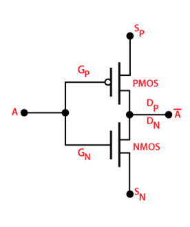
Here, G, S, and D specifies the Gate, Source, and Drain terminal of the NMOS and PMOS. The practical construction of CMOS is shown below: 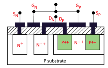
Let's consider the two states of the CMOS, when the input voltage (A) is 0 and 1. a) A in the above diagram is the input voltage that is fed to the NMOS and PMOS transistors. When the input voltage (A) = 0V, the PMOS conducts, and NMOS will remain in the OFF A' will become 1 when A is 0. Let's represent such condition in the form of NO and NC switches, as shown below: 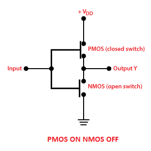
It means that the output voltage is considered as logic 1 because the PMOS switch is closed and the NMOS switch at the bottom is open. b) Similarly, when the input voltage A = 1, A' will be 0. In such a state, the PMOS will be OFF, and NMOS will conduct. Such state is represented below: 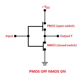
It means that the output is 0 when the input is 1. The output voltage is considered as logic 0 because the PMOS switch at the top is open and the NMOS switch is closed. CMOS Logic GatesCMOS logic gates are manufactured using the combination of NMOS and PMOS field-effect transistors. In the case of NMOS logic gates, we generally use NMOS depletion type transistors as the load resistance. In CMOS logic gates, we use a complementary structure in which one transistor acts as a load to the other transistor. The NMOS transistors are designed to work as positive logic elements, while PMOS works as negative logic elements. It means that both the transistors in a CMOS perform complementary logic functions. Features of CMOS Logic Gates The features of CMOS Logic Gates are listed below:
Types of CMOS logic gatesThe Complementary Metal Oxide Semiconductors are categorized as:
CMOS InverterThe CMOS inverter is formed by connecting the PMOS and NMOS transistors in cascade, as shown below: 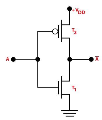
The top of the CMOS inverter is the PMOS transistor, while the bottom transistor is NMOS. The positive voltage of +VDD at the gate input of the NMOS transistors will turn it ON, while the same positive voltage at the gate input of the PMOS transistor will keep it OFF. Similarly, the voltage of 0 volts at the gate input of the NMOS transistors will keep it OFF, while the same 0 at the gate input of the PMOS transistor will turn it ON. It means that NMOS transmits logic 1 or VDD, and PMOS transmits logic 0. CMOS NANDCMOS NAND is a combination of NMOS NAND and PMOS NOR. It consists of an NMOS NAND gate with the PMOS NOR as its load. CMOS NAND gate can also include a PMOS NOR with the NMOS NAND as its load. It means that NMOS and PMOS transistors' combination in the desired manner forms a CMOS logic gate. The circuit diagram of CMOS NAND is shown below: 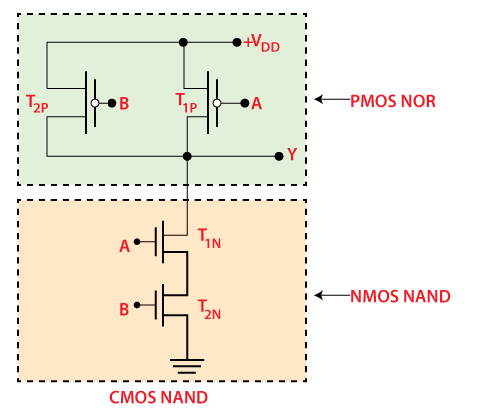
The input terminal of the transistors is A and B, as shown above. If A = 0 and B = 0, the NMOS transistors will remain off, and the two PMOS transistors will conduct. Consider the NOR table shown below:
It clearly shows that the output is 1 when the two inputs are 0. Hence, PMOS NOR will conduct. The output Y will be: Y = logic 1 = VDD Similarly, when both the input is 1, the NMOS NAND will conduct, and PMOS NOR will remain OFF. But, the output will be 0 because the power will pass to the ground. Consider the CMOS NAND table shown below:
CMOS NORCMOS NOR logic gate is a combination of NMOS NOR and PMOS NAND. The circuit diagram is shown below: 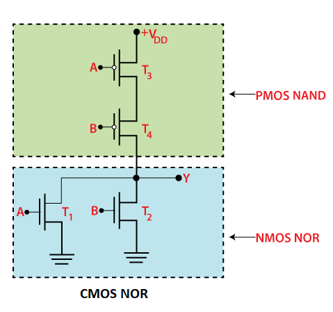
When both the input A and B are 0, NMOS NOR will remain OFF, and PMOS NAND will conduct. It means that transistors T1 and T2 will be OFF, while T3 and T4 will conduct. Thus, the output will be logic 1 when the voltage VDD reaches through the conduction of transistors T3 and T4. CMOS NOR will conduct only when both the inputs are 0 as discussed above. At all the other input conditions, the output will be 0, as listed below:
CMOS Operational AmplifiersThe CMOS structures can also be used as an amplifier when the operating point is fixed in the active region. Let's consider an example of a CMOS differential amplifier using constant current sources. 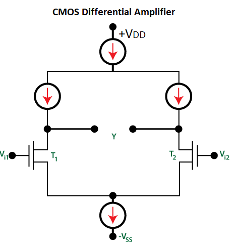
Advantages of CMOSLet's discuss the advantages of the Complementary Metal Oxide Semiconductor, which are listed below:
Applications of CMOSThe applications of CMOS are listed below:
CMOS vs. NMOSLet's discuss some differences between CMOS and NMOS for a better understanding. It will help us to analyze the applications of both these transistors in electronics.
Next TopicHall Effect
|
 For Videos Join Our Youtube Channel: Join Now
Feedback
- Send your Feedback to [email protected]
Help Others, Please Share


