| |

IC Fabrication ProcessIntegrated Circuits are the set of electronic circuits mounted on the small electronic chip. Large numbers of devices, such as MOSFETs (Metal Oxide Semiconductor Field Effect Transistor), transistors, microcontrollers, computer processors, etc., are created with the help of the fabrication process. The most preferred materials in the semiconductor industry for fabrication are silicon and germanium because of their stable structure. Other materials preferred in fabrication industries are carbon steel, silver, aluminum, magnesium, copper, wood, thermoplastics, resins, etc. Let's first discuss fabrication and its requirements in the semiconductor field. Fabrication is the process of constructing an industrial product. We can also define it as a set of methods to manufacture an electronic device or product. For example, silicon semiconductor chips, etc. In the case of metals, fabrication is a process used to convert the raw materials into the finished product. The smaller components manufactured by the fabrication process can be further used to make large electronic components. 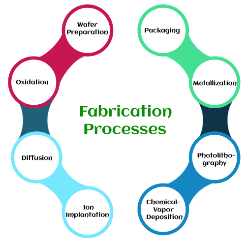
The basic fabrication processes of the Integrated Circuits are as follows:
Let's discuss the above processes in detail. Wafer PreparationA wafer is a thin material used for making various Integrated circuits and transistors. Wafer acts as a base for such devices. The material of a wafer is the semiconductor, especially crystalline silicon. The silicon crystals used for the wafer manufacturing are highly pure. The process of extracting pure metal from the melt is known as a boule. The impurities are further added to the molten state of the material in a specific amount to make it n-type or p-type. The wafer preparation is the first step for IC fabrication. It involves cutting, shaping, and polishing the wafer material to make it suitable for further fabrication. Some wafers are modified because of their sharp edges, irregular surface, and shape to convert them to the required wafer. OxidationOxidation is the process of adding oxygen. In a semiconductor, the oxygen and the silicon react to form silicon dioxide. The oxidation is carried out in furnaces at high temperatures upto 1250 degrees Celsius. Oxidation is classified as wet oxidation or dry oxidation. Both processes are widely used and have their own advantages and disadvantages. Wet oxidation is fast, while dry oxidation en has good electrical properties. Wet oxidation is also known as steam. Both types of oxidation have excellent electrical insulation properties. The deposition of silicon dioxide on the silicon wafer protects from many impurities. The dopants can be applied only to areas not covered with the SiO2. An example of oxide layer on the substrate is shown below: 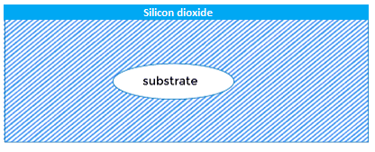
The oxidation process is one of the essential parts of the IC fabrication process and other VLSI (Very Large Scale Integration) devices. DiffusionDiffusion is a process of adding impurities atoms from a region with high concentration to a region of low concentration. The dopants or impurity atoms are added to the silicon (semiconductor material), which changes its resistivity. The process of diffusion is highly dependent on the temperature. It is carried out in high-temperature furnaces between 1000 degrees Celsius and 1200 degrees Celsius. The depth and width of the impurities depend on the temperature range and the timings. The high doping concentration improves the conductivity of a metal. The dopants can be of any state, solid, liquid, or gas. The preferred dopants are pentavalent impurities or n-type, such as antimony, phosphorous pentoxide, and arsine (gas). The trivalent impurities or p-type are gallium, indium, boron, etc. The diffusion cannot be used at the later stages. It is because the number of layers formed at the successive stages of the fabrication process might not be able to resist such high temperatures. For example, The boron or indium (trivalent impurities) diffusion on the n-type substrate forms a p-n junction. Diffusion is also a part of the process used to fill the lattice gap in the solids. Ion ImplantationThe ion implantation is a process of accelerating ions from the element to the solid target. The accelerated ions on the solid can change its properties. The ions are applied at a low temperature and high energy. The low temperature allows it to work at room temperature. But, the excess energy can also damage the crystal structure of the solid. 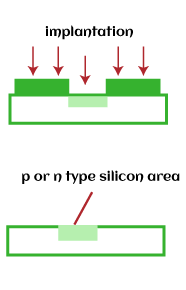
Ion implantation introduces impurity atoms in the crystal (semiconductor material). The accelerated atom gets embedded when it strikes the surface of the crystal. The energy and accelerating field voltage determine the depth of the penetration of the ions. The quantity of dopants can be controlled by adjusting the amount of ion concentration. Hence, ion implantation is more accurate due to the controlled current, voltage, and energy. The process is generally used when an accurate amount of impurity atoms is necessary for the device's operation. Chemical-Vapor DepositionCVD or Chemical Vapor deposition is used to produce high-quality solid materials. It produces thin films in the semiconductor industry. The process is carried out at a pressure below the atmospheric pressure, also known as vacuum deposition. The chemicals and vapors react to form solids on the surface of a substrate. The protective layers on the substrate, such as silicon dioxide, polysilicon, and silicon nitride, are deposited using the CVD process. For example, The reaction of silane gas, a molecule of silicon atom, with the oxygen on the surface of the silicon wafer results in the formation of SiO2 or silicon dioxide. The CVD process is not good enough compared to the thermally grown oxide but is enough to act as an insulator on the substrate. Its main advantage is the faster deposition rate at a lower temperature. CVD can be performed at very low pressures, low pressures, atmospheric pressures, sub-atomic pressures, and ultra high pressures. It depends on the chemical reactions involved in the process. Tungsten CVD is also used to create contacts or plugs on a semiconductor device. PhotolithographyPhotolithography is also known as optical lithography, using light to produce thin films. It is used to pattern thin films on the substrate, such as silicon wafers. It protects certain areas during successive fabrication processes (deposition, ion implantation, etc.). The types of light used to introduce mask patterns on the silicon wafer include UV light, X-rays, and extreme UV that emits at different frequencies. The most used type of light to produce the film is Ultra-Violet light. The silicon wafer or the substrate is first coated with a photoresist. On the photoresist layer, a mask pattern with the help of photolithography is applied to the silicon wafer. The exposed areas of the wafer become soft and can be removed. It creates a pattern on the wafer. The wavelength of each type of light determines the feature size impressed on the photoresist. Photolithography is somewhat similar to photography because the exposed area is patterned with help of the light. The incident light can be direct or projected through the lens. UV or Ultra-Violet LightUV light is exposed on the wafer with the help of a mask. It transfers the geometric design from the mask to the surface of the wafer coated with a photoresist. When the UV light falls on the exposed area on the substrate, the photoresist either breaks or hardens. The softened parts of the coating are further removed using the specific solvent. Photolithography is commonly used for the fabrication of microprocessors and solid-state devices. It can create a pattern of different sizes as small as nanometers. It is a quick, low-cost, and efficient method to create a substrate pattern in a single step. But, it is not ideal for irregular surfaces. In the case of complex IC circuits, the fabrication cycle can extend upto 50 times due to the microscopic structures. The light falling on the substrate can be UV or X-rays, as shown below: 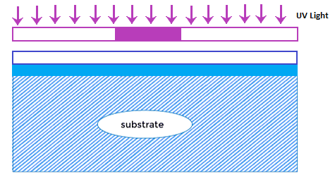
MetallizationMetallization is defined as the process of coating a metal layer on the metallic surface or non-metallic surface. The coating can be of aluminum, zinc, or silver. The metal coating in CMOS fabrication is aluminum, which protects the surface from external environmental factors, as dust, air, water, etc. 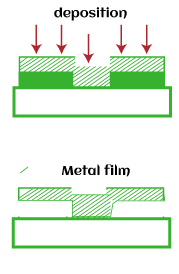
Metallization is also used to interconnect various components that form an Integrated circuit. The components can be resistors, capacitors, transistors, relays, etc. The metal layer is first deposited on the surface of the silicon wafer, as discussed above. After that, the required pattern or area for interconnected is etched, as shown below: 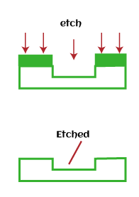
The metallization process uses chamber to apply metal layer. The wafer is placed inside the chamber, which coats the entire surface inside it. The thickness of the metal layer can vary depending on the requirements. PackagingPackaging is the last stage of the IC fabrication process. The finished silicon wafer or chips of various sizes with number of small components are tested electrically to recheck their working. The testing is performed using an automatic probing station. It is a cost effective testing machine that includes microwave and radio-frequency testing. The default circuits are separated from all the circuits. The good circuits are sent for packaging or headers. Packaging also assembles the ICs with other devices. IC is a component of a device. The external connections with the IC are packed together to form a device. We can also say that packaging is a connection between the manufacturing and end use of a device. It makes a product suitable for its end use. The package is finally sealed with epoxy or plastic to prevent it from atmospheric dust. It is performed under vacuum or an inert atmosphere, which prevents the material from oxygen that may get trap in the packaging. ConclusionLet's conclude the above IC fabrication processes. The IC fabrication starts with the wafer preparation, oxide layer deposition or a protective layer, introducing impurities into the wafer (n-type or p-type), implantation of ions to the surface of the crystal, CVD to produce thin films, photolithography (creating a mask pattern with the help of UV light), deposition of the metal for interconnections, and the packaging.
Next TopicClampers (electronics)
|
 For Videos Join Our Youtube Channel: Join Now
Feedback
- Send your Feedback to [email protected]
Help Others, Please Share


