| |

MOSFETMOSFET or Metal Oxide Semiconductor Field Effect Transistor is the transistor that operates under the applied electric field. The presence of an insulating oxide layer in MOSFET makes it different from other types of transistors. MOSFET is a type of FET (Field Effect Transistor). The other types of FET are MESFET (Metal Semiconductor Field Effect Transistor), MISFET (Metal Insulator Semiconductor Field Effect Transistor), and JFET (Junction Field Effect Transistor). Advantages of MOSFETLet's discuss some advantages of MOSFET over other types of FET.
The symbol of MOSFET is shown below: 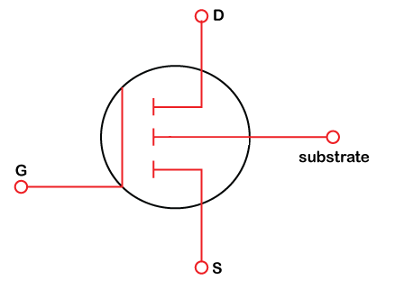
MOS (Metal Oxide Semiconductor) are similarly categorized as P and N types like BJT (Bipolar Junction Transistors). But, if we want to combine the P and N types, another category of MOS comes into a place called CMOS (Complementary Field Effect Transistors). MOSFET is an essential part of IC (Integrated Circuit) technology due to the following reasons:
IGFET (Insulated Gate Field Effect Transistor) is sometimes known as MOSFET. The gate terminal of the MOSFET is insulated with a thin layer of insulating material of silicon dioxide. MOSFET is used in a wide range of applications, such as:
Operation of MOSFETLet's discuss the MOSFET and its operation in detail. MOSFET has four terminals called Drain (D), Source (S), Gate (G), and Substrate (SS). The role of the gate is to control the flow of current or charge carriers. The role of the drain is to receive the charge carriers that are ejected by the source. The drain terminal is always applied with positive potential with respect to the source. We can apply either a positive or negative potential at the gate. The MOSFET is categorized as p-type and n-type depending on the substrate. If a p-type semiconductor is used as a channel, the substrate will be opposite polarity, i.e., n-type semiconductor. Such type is known as p-type MOSFET. If an n-type semiconductor is used as a channel, the substrate will be of p-type. It is known as n-type MOSFET. The n-channel MOSFET is called NMOS, while p-channel MOSFET is known as PMOS. The name Metal Oxide Semiconductor signifies the insulating material called silicon dioxide, a metal oxide. The channel is present between the drain and the source. When we apply negative bias at the gate terminal, the MOSFET is known as the depletion type MOSFET. When the positive bias is applied, it is called an enhancement type MOSFET. Let's discuss these types in detail. Types of MOSFET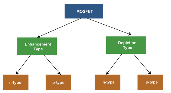
There are two types of MOSFET, which are listed below:
Depletion Type MOSFETThe voltage applied at the gate depletes the channel, due to which it is known as Depletion-type MOSFET. Depletion Type MOSFET is further categorized into:
In n-type depletion MOSFET, the negative voltage at the gate decreases the drain current. While in p-type depletion MOSFET, the positive voltage at the gate decreases the drain current. Let's discuss this in detail. N-channel depletion type MOSFETConstruction The symbol of the n-channel MOSFET is shown below: 
The structure of the n-channel depletion type MOSFET is shown below: 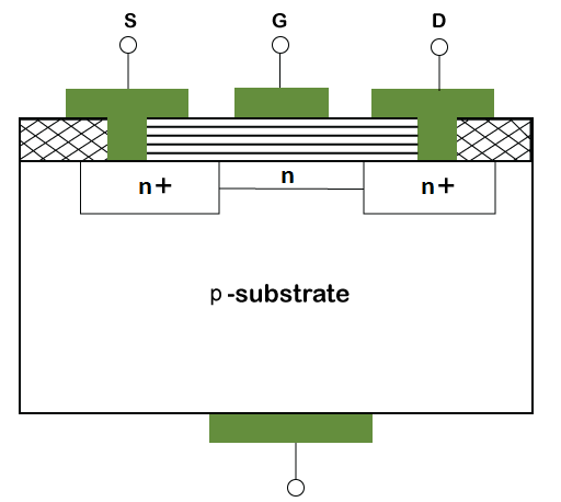
Let's understand the structure of the n-channel depletion type MOSFET.
Principle The gate terminal of the MOSFET can be applied either positive or negative bias. When the negative bias is applied at the gate terminal, it repels the electrons in the n-channel. The electron moves towards the substrate. It results in the depletion of the channel due to the movement of charge carriers. Working When the negative bias is applied to the MOSFET's gate end, it repels the negatively charged ions of the n-channel (the same charge repels) and attracts its minority carriers (holes). The negative charge ions move towards the substrate. The minority carriers settle near the silicon oxide layer of the MOSFET. The holes present in the substrate attract these negatively charged ions (opposite charges attract). Due to the movement of charge carriers, the channel region gets depleted. Such depletion affects the flow of drain current due to decreased charge carriers. The more negative the gate becomes, the lesser will be the drain current (ID). The n-channel MOSFET after the depletion will appear as: 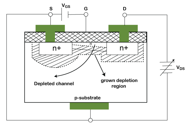
P-channel depletion type MOSFETConstruction The symbol of the p-channel MOSFET is shown below: 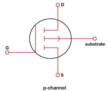
The structure of p-channel depletion type MOSFET is shown below: 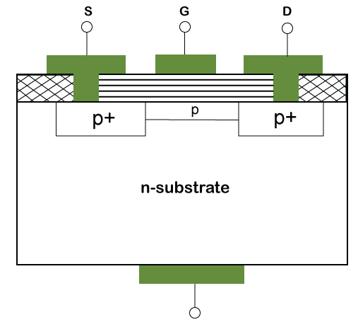
The structure of p-type depletion MOSFET is similar except for the reversed polarity. Consider the below points:
Principle When the positive bias is applied at the gate terminal, it repels the majority charge carriers of the p-channel (holes). Due to the movement of charge carriers away from the channel, it gets depleted. Such depletion affects the flow of drain current due to decreased charge carriers. Working When the positive bias is applied to the MOSFET's gate end, it repels the positively charged ions of the p-channel (the same charge repels). The positive charge ions move towards the substrate. The electrons present in the n-type substrate attract these positively charged ions (opposite charges attract). Due to the movement of charge carriers, the channel region gets depleted. Drain CharacteristicsThe drain current variation with drain-to-source voltage is known as drain characteristics. The drain current variation with gate-to-source voltage is known as transfer characteristics. Here, we will discuss the drain characteristics of both p-type and n-type depletion MOSFET. 1. N-type Depletion MOSFET Gate-to source voltage (VGS) is equal to pinch-off voltage for drain current to be zero. VGS = -VP (off state) 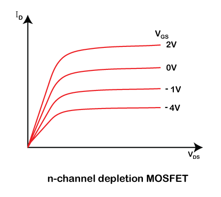
2. P-type Depletion MOSFET Positive values result in reduced drain current. The pinch-off voltages for zero drain current in written as: VGS = +VP (off state) 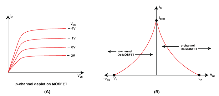
Enhancement Type MOSFETThe difference between enhancement and depletion type MOSFET is that it has no channel between source and drain. It means that enhancement type MOSFET has two diffusion windows. Enhancement Type MOSFET is further categorized into:
Let's discuss this in detail. N-channel enhancement type MOSFETConstruction The symbol of the n-channel MOSFET is shown below: 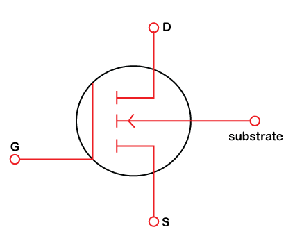
The structure of the n-channel enhancement type MOSFET is shown below: 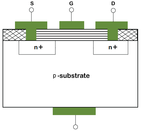
Let's understand the structure of the n-channel enhancement type MOSFET.
Principle When the positive bias is applied at the gate terminal, it repels the majority charge carriers of the p-substrate (holes). It is due to the absence of a channel between the source and drain except the two diffusion windows. Working The positive bias is applied to the gate end of the MOSFET, which repels the majority carries holes away from the region between drain and source. It leaves the negative acceptors with few minority carriers in that region. The positive gate bias also attracts electrons from the source window. Hence, a new region of negative charge is developed between the drain and source region. The drain current flows in this region with the increase in VDS. The region formed between the drain and source is also known as the inversion layer due to the formation of the n-type channel in the p-type substrate. MOSFET will now appear as: 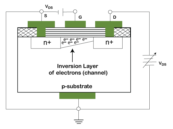
Increase in drain voltage results in the reduction of channel width from the drain side due to sudden saturation of negative charge carriers. P-channel enhancement type MOSFETThe working of p-channel enhancement MOSFET is opposite to that of n-channel enhancement MOSFET. Construction The symbol of p-channel enhancement MOSFET is shown below: 
The structure of p-channel enhancement type MOSFET is shown below: 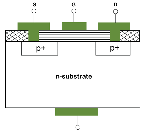
Let's understand the structure of the p-channel enhancement type MOSFET.
Principle When the negative bias is applied at the gate terminal, it repels the majority charge carriers of the n-substrate (electrons). It is due to the absence of a channel between the source and drain, except for the two diffusion windows. Due to the reverse polarity, drain current increases with the increase in negative gate voltage. Working The negative bias is applied to the MOSFET gate end, which repels the majority of carries electrons away from the region between drain and source. It leaves the positive donor ions with few minority carriers in that region. The negative gate bias also attracts holes from the P+ source windows. Hence, a new region of positive charge is developed between the drain and source region. 1. N-type enhancement MOSFET The conductance through the inversion layer is directly proportional to: VGS -VT, where VT is the threshold voltage. When VDS is applied, ID flows according to the density of electrons in the channel. The increase in VGS voltage results in an increase in the density of electrons. If, VGS < VT: ID will be equal to zero. VGS = VT: ID begins to rise due to the induced channel formation. 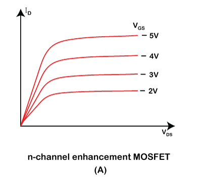
2. P-type enhancement MOSFET The transfer characteristics are reverse from n-type. ID (Drain current) increases only when -VGS exceeds VT. It is shown below: 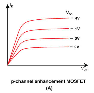
Important terms and DifferencesLet's discuss some important terms and differences between the types of transistors. Depletion type MOSFET vs. Enhancement type MOSFETWe have already discussed the depletion and enhancement type of MOSFET in detail. Let's discuss some main differences.
MOSFET vs. BJT
MOSFET vs. JFET
MOSFET vs. MESFET
MISFETMISFET stands for Metal Insulator Semiconductor Field Effect Transistor. The structure of MISFET is similar to that of JFET. It has three terminals called Drain (D), Source (S), and Gate (G). It is a combination of metal-insulator-semiconductor that constructs a field effect transistor. The voltage applied at the gate electrode controls the drain current. The insulator is used to isolate the gate from the channel. Hence, the device is known as Metal Insulator Semiconductor Field Effect Transistor. MISFET is used in various applications, such as power amplifiers, frequency converters, etc. CMOSCMOS or Complementary Metal Oxide Semiconductors are manufactured by the combination of NMOS and PMOS Filed-Effect Transistors. In CMOS structures, PMOS act as the load to NMOS transistors. NMOS FET is designed to operate as the positive logic elements, and PMOS FET is designed to operate as negative-logic elements.
Next TopicPrometheus Monitoring
|
 For Videos Join Our Youtube Channel: Join Now
Feedback
- Send your Feedback to [email protected]
Help Others, Please Share


