| |

PNP TransistorsPNP is a type of Bipolar Junction Transistors (BJT). P signifies the p layer, and n signifies the n layer. P layer comprises of majority carriers holes and n layer comprises of majority carriers electrons. BJT is categorized into two types called PNP and NPN transistors. It is due to the two types of current flowing in it, known as input and output current. Such transistors are called current-controlled devices. PNP transistors are categorized as bipolar devices because current flows between two points than a single in the presence of an electric field. The PNP transistor has three regions, namely emitter, base, and collector. The emitter side is known as the input circuit, and the output side is known as the output circuit. Let's discuss its construction and work in detail. ConstructionPNP is a transistor where an n-type semiconductor slap is sandwiched between two p-type semiconductor slabs. Transistors are generally fabricated using silicon or germanium semiconductors. The fabrication is present in the form of an emitter, base, and collector. The block diagram of the PNP transistor is shown below: 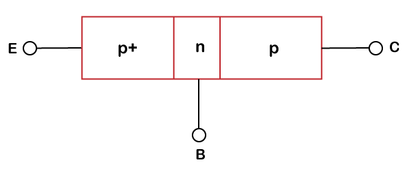
Here, p+ signifies that the emitter junction is heavily doped. The role played by the emitter and collector cannot be interchanged. The collector region in transistors is usually large as compared to other regions. It is because the collector is required to dissipate more heat. The symbol of the PNP transistor is shown below: 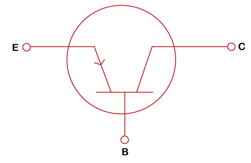
The arrow in the above PNP symbol depicts the flow of input emitter current. In the case of the PNP transistor, the emitter current flows from the emitter to the base. The base region of the PNP transistor is small with very light doping. The emitter region is heavily doped to offer a large number of charge carriers. The collector is doped at an intermediate level as compared to the emitter and base. FunctionLet's first discuss the functions of the three regions of the PNP transistor. The function of the emitter is to inject the electrons into the base region. The base region is very thin passes most of the charge carriers towards the collector. The collector's role is to collect the charge carriers and contribute to the flow of current in the circuit. Hence, the two junctions of the transistor play an essential role in the flow of charge carriers. There are two junctions between the three layers of the PNP transistors. These junctions are called emitter-base junctions and collector-base junction. Thus, we can say that the PNP transistor looks like the combination of two p-n junction transistors connected back-to-back. WorkingLet's discuss the working of the PNP transistors. Connection setupThe structure of the biased PNP transistor is shown below: 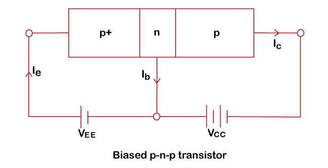
The direction of currents is in the same direction as the direction of the flow of holes or opposite to the flow of electrons. The emitter-base junction is forward bias, while the collector-base junction is reversed biased. The positive terminal of the battery is connected to the p-type semiconductor, which forms forward bias. The forward biasing of the emitter-base junction provides the negative potential to the n-type base region. The positive end of the voltage source Vcc is connected to the n-type base region, and the negative terminal is connected to the p-type collector region. The voltage source (VE) connected to the p-type emitter repels each other due to the same polarity. WorkingThe connection setup of the PNP transistor is discussed above. Let's discuss it's working. The connection of the positive terminal of the voltage source VE to the p-type emitter region forces holes to move from the emitter region to the base region. It is because the same charge repels. The base region is thin and lightly doped. Hence, it passes 95% of the positive charge carriers (holes) to the collector region. Only 5% of the left holes recombine with the majority charge carriers of the n-type base region, constituting the base current. The collector region is also p-type, which consists of majority carriers holes. The collector also receives 95% of the holes from the base region. This 95% of the transferred holes move along with the majority charge carriers of the collector region to execute large collector current. Consider the current components in the p-n-p transistor. It will help us to clearly understand the concept and directions of the current flowing in the transistor. It is shown below: 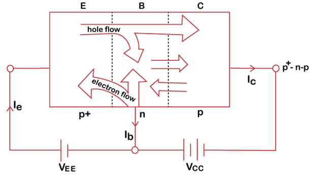
Transistor current in p-n-p transistorsThere are three types of primary currents flowing in the transistors, namely emitter current (Ie), base current (Ib), and collector current (Ic). The direction of these three currents is shown below: 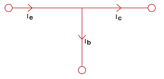
Let's discuss a short description of these currents flowing in a PNP transistor. Emitter currentThe total emitter current is the sum of currents flowing due to the majority carrier's holes and the minority carrier's electrons. Base currentThe total base current flows due to minority carriers holes of the base region. Collector CurrentThe total collector current is the sum of currents flowing due to the number of majority carriers' holes and minority carrier's electrons. Leakage currentsThere are two types of leakage current flowing in the transistor. These two currents flow due to the minority charge carriers available in the transistors, namely emitter-base junction leakage current and collector-base junction leakage current. The leakage current flows only in the reverse-biased junction. Thus, we can say that minority charge carriers present in the collector are responsible for leakage current flow. Emitter Injection EfficiencyWhen the emitter-base region is forward biased, the width of the depletion is reduced. It results in a reduced amount of space-charged carriers in the depletion region. The reduced depletion width promotes the diffusion process. It results in the rapid diffusion of majority charge carriers across the depletion region. Thus, the emitter injection efficiency is calculated as the ratio of the majority carrier current to the emitter's total current. 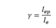
Base transportation factorsThe base transportation factor is represented as B. The injected charge carriers through the emitter into the base region are majority carriers according to the emitter. The same charge carriers are minority charge carriers according to the base. It is because the base is the n-region. The charge carriers in the base region may also include some extra charge carriers generated thermally. The base region's small width does not hold the charge carriers, further moving towards the collector region. It also lacks a recombination process in the region. The base transportation factor is defined as the ratio of collector current to the emitter current. The collector current is generated due to the total amount of charge carriers in the collector region. The emitter current is produced due to the majority of carriers present in the emitter region. The maximum value of the base transportation factor can be 1. B = Ic/Ie Where Ic is the collector current Ie, is the emitter current. When B < 1 It depicts that the collector current is less than the emitter current. It can happen due to the following reasons:
Current gainThe current gain of the p-n-p transistor is defined as the ratio of output current to the input current. By varying the emitter current or base current, we can control the collector current in the transistor. There are two types of current gain, namely common base current gain and common emitter current gain. Let's discuss this in detail. Common base current gainThe variation in the output collector current with respect to the input base current is known as common base current gain. It is represented as: 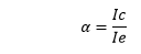
The value of the common base current ranges between 0.9 and 0.99. Common emitter current gainHere, the base junction is used as the input. The output collector's variation to the input base current is known as the common-emitter current gain. It is represented as: 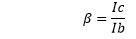
Relation between Current gainsHere, we will discuss the relation between the two current gain discussed above. The two current gains are common base current gain and common emitter current gain. The relation between these two current gains can be represented as: 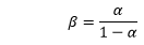
Terminal resistance values for p-n-p transistorsWe know that the emitter-base region of the p-n-p transistor is forward biased, and the collector-base region of the transistor is reverse biased. A small change in negative voltage across the base of the p-n-p transistor and the output current will convert the state of the transistor from OFF to ON. It results in the flow of emitter-collector current. PNP vs. NPN transistorsLet's discuss the differences between the p-n-p and n-p-n transistors. Consider the below table:
Next TopicToolbar in Computer
|
 For Videos Join Our Youtube Channel: Join Now
Feedback
- Send your Feedback to [email protected]
Help Others, Please Share


