| |

SemiconductorThe conductivity property of a semiconductor lies between the conductors and insulators. It means that the conductivity of semiconductors is not as good as the conductivity of metals, but not as poor as insulators. We can control the conductivity of a semiconductor by introducing impurities into its crystal structure. The applications of semiconductors include various electronic devices, such as ICs (Integrated Circuits), diodes, and transistors. The common examples of semiconductors include Silicon and Germanium. Here, we will discuss the following topics: Charge Carriers of Semiconductor Band Gap Energy of Semiconductors Direct and Indirect Semiconductors Recombination and carrier generation in semiconductors Advantages and disadvantages of Semiconductors Semiconductor MaterialsThe semiconductor materials are generally solid at room temperature. The commonly used solids are found in the powder or polycrystalline form. Some of the available crystalline materials also exist in nature form, such as diamond. Nowadays, crystals can be developed using the human-made process. A perfect crystal is regular throughout its structure and is rather difficult to achieve. Sometimes, a created crystal ends up with built-in defects. But, it is interesting to know that defective crystals are also useful in the semiconductor materials. Let's start with the semiconductor materials and their properties. Among all the types of semiconductor materials, Silicon, Arsenic, Gallium, and Germanium are the most common used materials that are used in making different types of semiconductor devices. Alloy materials are also preferred as the semiconductor materials. Silicon and Germanium are the basic elemental material used for making various devices. A semiconductor compound GaAs is also a useful material. Consider the below table that displays the types of semiconductors with the examples.
Where, Al- Aluminum As- Arsenic B- Boron C- Carbon Cd- Cadmium Ga- Gallium Ge- Germanium In- Indium N- Nitrogen P- Phosphorous S- Sulfur Sb- Antimony Se- Selenium Si- Silicon Te- Tellurium Zn- Zinc The above names are the full form of the semiconductor materials mentioned in the above table. Now, we will discuss the properties of the most common materials, i.e., Silicon and Germanium. SiliconThe atomic number of silicon is 14, and it is represented with the symbol Si. The availability of silicon in Earth's crust is large, which allows its applications for thousand years. In 1906, a radio pioneer and an American engineer named Greenleaf Whittier Pickard invented the first silicon device. The device was named as a silicon radio crystal detector. In 1954, the first silicon junction transistor was fabricated by the American chemist named Morris Tanenbaum at the Bell Labs. Around the late 1950s, Germanium became the popular semiconductor material than silicon. It was also preferred as a material for transistors. Silicon is scarcely found in its pure form in the Earth's crust. The first abundant element available in the Earth's crust is oxygen. After it comes to the element silicon, it means that silicon's rank lies in the fiftieth number as per the abundant materials in the Earth's crust. GermaniumThe atomic number of Germanium is 32, and it is represented with the symbol Ge. The performance of the Germanium is better than silicon due to its high carrier mobility. Electron mobility is the semiconductor property that shows movement of an electron in the semiconductor under the applied electric field. The pure form of germanium is a semiconductor. The appearance of Germanium is similar to that of silicon. The rank of Germanium lies in the fiftieth number as per the abundant materials in the Earth's crust. It means that Germanium rarely appears in high concentrations. At present, the applications of Germanium lie in solar cells, LED, etc. Both silicon and germanium can react with oxygen to form complex oxides. History of SemiconductorsThe history of semiconductors started around the invention of materials, rectifiers, and transistors' electrical conductivity.
History of devices based on semiconductorHere, we will discuss the invention of semiconductor devices.
Energy bandgap of the SemiconductorThe atoms of solid materials are held together by the forces of repulsion and attraction. It maintains a balance by keeping the atoms at a specific distance known as inter-atomic distance. This distance is not the same for all types of solids. The energy level diagram of an atom is shown below: 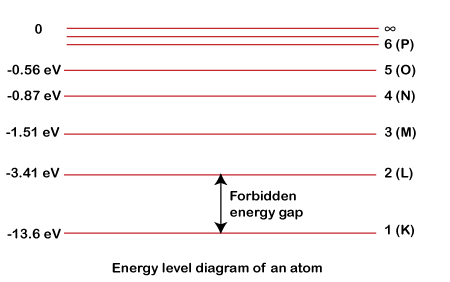
Here, K, L, M, N... is the discrete energy levels that are separated by the number of energy gaps. As shown, the forbidden energy gap between the two energy levels keeps on decreasing as we go upwards. It is the case of an isolated atom. Now, let's consider the case of solids. The energy levels of the atoms in a solid are based on quantum mechanics. It clearly explains that the discrete energy levels in solids are closely spaced, which are called bands. The band in solids is separated by a forbidden energy gap (Eg), as shown below: 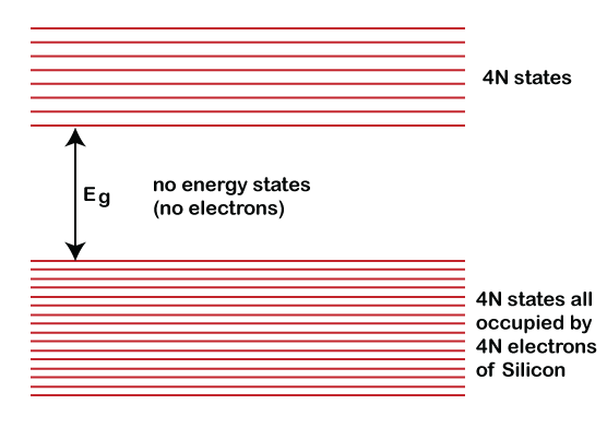
Here, we will discuss valence and conduction bands in detail. Conduction Band The conduction band comprises of the mostly empty energy states. The excited electrons from the valence band jump into the conduction band. The electrons present in the orbits of the conduction band are free to move. The movement of the electrons generates the current. When the electrons cannot jump to the conduction band, the materials lack conductivity. In a given band, an electron may transfer from one energy state to another. Valence Band The valence band consists of the band of electrons that jumps to the conduction band when it gains energy. A bandgap is the energy gap between the valence band and conduction band, as shown below: 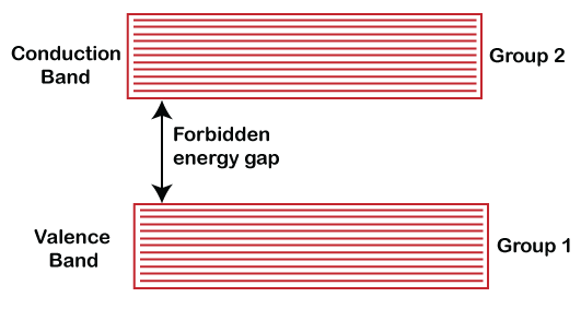
Now, let's clearly understand the forbidden energy gap in semiconductors. We will also discuss the energy gap in the case of insulators and metals. In any solid, the applied voltage generates the magnetic field. The electrons of the solid will experience acceleration. F = ma Where, F is the force generated by the magnetic field a is the acceleration As soon as the electrons move in the higher energy states, the electrons' energy starts increasing in the case of empty energy states. For example, if some of the energy states (like 4N) in the valence band are filled, there will be no energy available for electrons' movement in the valence band. In the conduction band, the available empty energy states are greater, but there are no electrons. Let's consider a case of silicon at 0K. The applied magnetic field on the silicon at 0K will result in no electrons movement and no current. It means that silicon at 0K acts as an insulator. The increase in temperature will cause the electrons to move due to the increased thermal energy with the temperature rise. Some electron possesses sufficient energy to move, while some electrons possess extra energy that may be greater than the forbidden bandgap energy or Eg. The extra energy allows the electrons to jump to the conduction band. The electrons will jump where there are more empty energy states. We will now consider the same case of silicon, but at room temperature (around 300K). A reasonable amount of electrons is present in the conduction band of the Silicon at room temperature. The applied electric field will provide acceleration to the electrons in the conduction band. The electrons will gain energy and move to the available empty energy states in the conduction band. It will acquire velocity and generates a small amount of current. Hence, silicon at room temperature is not an insulator. It starts conducting due to small amount of current. The electrons which have jumped from the valence and to the conduction band are smaller in number. It means that silicon is not a good conductor of electricity. Hence, it Silicon is termed as a Semiconductor. The Forbidden energy gap of Silicon is 1.1eV. Let's consider another case for better understanding. Here, we will discuss the reason for the diamond being insulator at room temperature. The Forbidden energy gap of the diamond is 5.47eV. At room temperature, the electrons present in the diamond's valence band could not jump to the conduction band. Hence, diamond is considered as an insulator at room temperature, while silicon is a semiconductor. But, at very high temperatures, a diamond can become a semiconductor. Band Gap of ConductorsThe valence band and the conduction band in the conductors overlap each other. It means that the Bandgap of the conductors is 0 due to the overlapping of these two bands. The conduction band consists of a large number of electrons. It allows the flow of heavy current under the applied electric field. The bandgap diagram of the conductor is shown below: 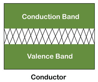
Band Gap of InsulatorsThe materials with a bandgap greater than 5.0eV are considered as Insulators. It is the Bandgap generally at room temperature. The electrons at room temperature do not gain sufficient energy to jump from the valence band to cover the forbidden energy gap and reach the conduction band. The bandgap diagram of insulators is shown below: 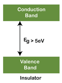
Band Gap of SemiconductorsThe materials with a bandgap less than 3.0eV are considered Semiconductors. The valence electrons do not gain enough energy to jump to the conduction band and participate in the current process. Since the Bandgap is less than the insulators, some of the electrons can participate in the current process. It results in a small current flow. Hence, the conductivity of semiconductors lies between the conductors and insulators. The popular semiconductors materials include Silicon (1.1 eV), Germanium (0.7 eV), and GaAs (1.43eV). The bandgap diagram of semiconductor is shown below: 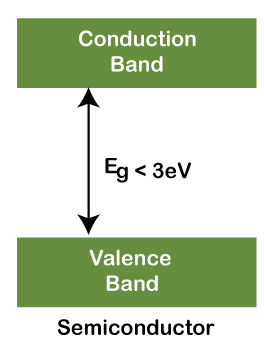
Bonds in SolidsBonds in solids can be categorized as Ionic, Covalent, and Metallic bond. The motion of electrons in the ionic and covalent bond is restricted. The electrons in the case of the metallic bond are free to move. Let's discuss a short description of all three types of binds. Ionic BondThe electrons in the outermost orbit of an atom and transferred to the other atom's outermost orbit to create a stable configuration. Features of Ionic Bonding
Covalent BondIn covalent bonds, the neighboring atoms share their valence electrons to form strong covalent bonds. It means no transfer of electrons from one atom to another, like an ionic bond. The Silicon (Si) crystal has a covalent bond between its atoms. Consider the covalent bond formation in the silicon atom, as shown below: Features of Covalent Bonding
The optical properties are quite similar to that of ionic crystals. Metallic BondThe electrons are loosely bound to the atoms in the case of metals. The atoms with one atom in the outermost shell are metallic, while atoms with four electrons in the outermost shell are less metallic. Similarly, more than five atoms (six or seven) in an atom's outermost shell can cause it to lose the metallic properties. Features of Metallic Bonding
Types of SemiconductorThere are two types of semiconductors, intrinsic and extrinsic semiconductor. Let's discuss this in detail. Intrinsic SemiconductorWe know that Silicon at room temperature has no electrons in the conduction band. The semiconductor that is free from any crystal defect and impurities are called intrinsic semiconductors. The increase in temperature can result in the electrons to jump from the valence band to the conduction band after gaining thermal energy. The jump of the electrons leaves a hole in the valence band. An EHP (electron hole pair) is thus created in this process. The increase in temperature can create more holes in the valence band. At a certain temperature the number of holes becomes equal to the number of electrons in the valence band. Charge carrier concentration in Intrinsic At 0K, the conduction band of the intrinsic semiconductor consists of no charge carries. The rise in temperature causes the electrons to jump from the valence band to the conduction band. Extrinsic SemiconductorThe semiconductors with impurities and defects are called extrinsic semiconductors. The process of introducing impurities in the semiconductor is called doping. The doping helps in increasing the conducting properties of a semiconductor. It also provides additional energy levels in the forbidden energy gap. Electrons at the added level are so close to the valence band and conduction band that they can easily jump to these bands to increase their population. A given amount of doping increases the population of electrons in the conduction band. Such doped semiconductors are termed extrinsic semiconductors. Ewe can convert the intrinsic semiconductor into an extrinsic semiconductor by applying impurities or doping. An extrinsic semiconductor is further categorized into P-type and N-type semiconductors. Let's discuss the above types of semiconductors in detail. P-type The application of trivalent impurities on the intrinsic semiconductor can result in the formation of the P-type extrinsic semiconductor. Trivalent means the atoms with doping valency of 3. It generally donates excess holes due to its positive charge. Trivalent impurities are often known as acceptor impurities. The acceptor energy level of the P-type is close to the valence band, as shown below: The examples include Aluminum and Boron. It is called acceptor impurity because the atoms can easily accept electrons from the neighboring atom due to the vacancy. The majority of carriers in a P-type semiconductor are holes. It means that holes are much greater than the number of electrons. N-type The application of pentavalent impurities on the intrinsic semiconductor can result in the formation of a N-type extrinsic semiconductor. Pentavalent means the atoms with five electrons in the outermost shell. Pentavalent impurities are often known as donor impurities. It is called a donor because it shares a free electron with the semiconductor. The donor energy level of the N-type is close to the conduction band. The examples include arsenic and phosphorous. The majority of carriers in a N-type semiconductor are electrons. It means that electrons are much greater than the number of holes. Charge Carries in the SemiconductorThe charge carriers of a semiconductor are electrons and holes. The electrons possess a negative charge, and holes possess a positive charge. The movement of electrons determines the flow of charge in a semiconductor. But, it does not mean that holes do not participate in the conduction process. The minority charge carriers mean the smaller number of carriers present in the semiconductor material. The majority carriers signify the greater number of charge carriers. The flow of charge depends on the majority of charge carriers. Let' discuss the charge carriers in the p-type and n-type semiconductors. The majority carriers in the p-type semiconductor are holes, while the minority charge carriers are electrons. The majority carriers in the n-type semiconductor are electrons, while the minority charge carriers are holes. Doping in SemiconductorsThe Bandgap of the semiconductor is small as compared to the Bandgap of the conductor. Doping is a process to add impurities to the semiconductor, which increases the semiconductor material's conductivity. 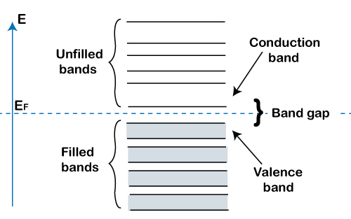
An impurity added to the semiconductor materials is known as Dopant. For example, the addition of pentavalent impurities, such as arsenic, increases the material's conductivity by contributing free electrons. The increase in the number of doping concentration results in higher conductivity. It is due to the presence of extra charge carriers. Let's first discuss the effect of doping on the materials. It is listed below: SiliconSilicon is the essential semiconductor material for the semiconductor industry. Boron and phosphorous are the two important impurities that can be applied on the silicon. Let's discuss how the trivalent Dopant (boron) and Pentavalent Dopant (phosphorous) contribute to doping with the silicon atom. The diffusion rate of boron and silicon is fast. Boron Boron is considered as p-type doping that has three valence electrons. It means that it is missing the fourth valence electron. The silicon atom has four valence electrons. When boron is doped on the silicon, it creates a hole in the silicon lattice. The holes created in the lattice are free to move. Thus, a p-type semiconductor is formed. Phosphorous Phosphorous is considered as n-type doping that has fie valence electrons. It means that it has one extra valence electron. The silicon atom has four valence electrons. When phosphorous is doped on the silicon, it forms a covalent bond with the silicon's four electrons. The extra electrons become unbounded to the atoms in the silicon lattice. Thus, an n-type semiconductor is formed. Effect of doping on the semiconductorsThere are two types of materials on which the doping can be applied. We know that applying doping on the intrinsic materials results in the formation of extrinsic materials. Let's discuss the effect of doping on the types of extrinsic semiconductor materials. P-type consists of majority carry holes. The p-type doping signifies the doping of trivalent impurities. N-type consists of a majority of carrier's electrons. The n-type doping signifies the doping of pentavalent impurities. The p-type dopants are boron, gallium, indium, and Aluminum. Boron doping is popular in CMOS (Complementary Metal Oxide Semiconductors) technology. Aluminum doping is preferred for deep p-diffusions. The p-type dopants are Antimony, lithium, arsenic, bismuth, and phosphorus. The antimony doping is preferred for its use in buried layers. Arsenic doping is popular in VLSI (Very Large Scale Integration) circuits. The other types of dopants are Nitrogen, Xenon, Gold, Platinum, etc. Nitrogen doping is popular for growing defect-free silicon crystals. Dopant materials for semiconductors Here, we will discuss the doping materials preferred for different types of semiconductors. The doping materials preferred for Group IV semiconductors, such as silicon germanium, diamond, etc., are the trivalent or acceptors and donors. The acceptors are the elements of group III. The donors are the elements of group V of the periodic table. Direct and Indirect SemiconductorsThe transition in such types of semiconductors is radiative. It means that the direct and indirect semiconductor depicts an electron's fall from the conduction band to the valence band when it loses energy. The energy that the electron loses while coming from the conduction band to the valence band is given out as radiation corresponding to the bandgap energy (Eg). Let's discuss direct and indirect semiconductors in detail. Direct SemiconductorsThe semiconductors where the conduction band is situated just above the valence band are called direct semiconductors. The diagram of direct semiconductor is shown below: 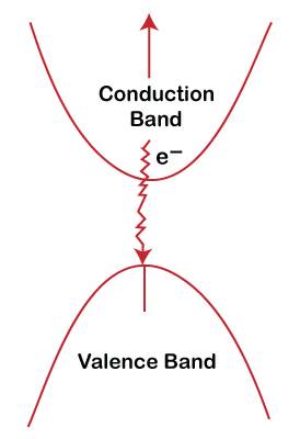
In the above diagram, the conduction band energy parabola's energy minima are just above the valence band energy parabola's maxima. It means that the transition in such cases is direct. The direct semiconductors are a good source of optical radiations. Indirect SemiconductorsThe diagram of the indirect semiconductor is shown below: 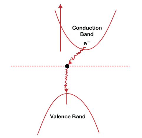
In this case, the conduction band is shifted to the right side, and its minima have a positive value. Here, an electron transition from the conduction band to the valence band is a two-step process. It first locates a lower energy level (Et). The electron loses energy and comes to the energy level Et. The energy lost in this process is non-radiative and comes out as heat. Under appropriate conditions, the electron now at energy level Et may fall to a valence band release a photon. The indirect semiconductors can be used as a controlled photon radiator. Mixed SemiconductorA semiconductor, which is a mixture of both direct and indirect semiconductors called a mixed semiconductor. The diagram of mixed type semiconductors is shown below: 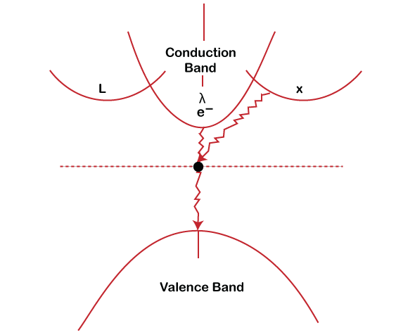
Recombination and carrier generation in semiconductorsRecombination and carrier generation signifies the elimination and generation of charge carriers. The charge carriers are electrons (negatively charged) and holes (positively charged). These two processes are the basics of different electronic devices, such as LED (Light Emitting Diodes), photodiodes, etc. The transition of an electron between the valence band (lower band or energy state) and the conduction band is based on the generation of electron-hole pair. Let's discuss the recombination and carrier generation process in semiconductors. Carrier generationCarrier generation signifies the generation of charge carriers. The transition of the electrons in the case of carrier generation is from the valence band. The carriers can be generated by the light interacting on the materials or the applied electric field. It generates a pair of free carriers in the semiconductor materials. The electrons across the bandgap can be excited when sufficient energy is applied to it with an external source. It lowers the resistance of the material by generating extra charge carriers. RecombinationRecombination signifies the elimination of charge carriers. The transition of the electron is reversed as compared to the transition in carrier generation. It means that the transition of the electron is from the conduction band (upper band) to the valence band. In the recombination process, the jump of electrons (after the electron excitation) from the conduction band to the valence band results in the release of energy in the form of photons. The energy of the released photons can be less or more than the energy that was initially absorbed. The phenomenon of light generation by LEDs is based on such a concept, where the photons are released in the form of light. The released energy can be in the form of heat or light. When the recombination of charge carriers release phonons instead of photons, the energy is released in the heat. 
Properties of SemiconductorThe properties of a semiconductor determine the behavior of the semiconductor materials. Let's discuss the different properties of a Semiconductor.
Advantages and disadvantages of a semiconductorLet's discuss the advantages and disadvantages of the semiconductor. Advantages of SemiconductorLet's discuss the advantages of semiconductors that made them popular for use in various applications. These are listed below:
Disadvantages of SemiconductorThe disadvantages of semiconductor are listed below:
Applications of Semiconductor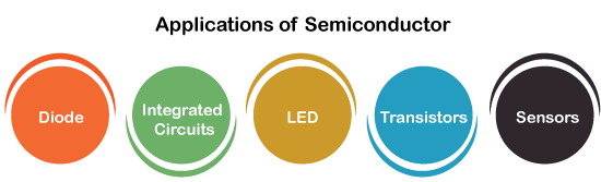
The use of semiconductors in solids allows the devices to operate at low voltage and less power. Hence, most of the electronic devices are created using semiconductor materials. Let's discuss the various applications of semiconductors in detail. DiodeIt is the simplest form of electronic device that is based on semiconductors. The diode is a type of device that consists of joined P and N junctions. It allows the current to move in one direction as compared to the other direction easily. It means it blocks one direction so that the current can easily flow through the other. Silicon is the common semiconductor material used as the diode material. Integrated Circuits (ICs)The Integrated Circuits or ICs are used in almost every electronic device, such as radio receivers, calculators, sensors, timers, etc. IC comprises a thin silicon chip with electronic items, such as transistors, diodes, etc. LEDsLEDs are also created using the semiconductor material. It emits light when current passes through its circuitry. The applications of LEDs include ring lights, flashlights, decorative lights, household bulbs, etc. The recombination of holes (positive charged) and electrons (negative charged) in a semiconductor is responsible for generating lights in LED (Light Emitting Diodes). TransistorsTransistors are created using semiconductor materials. It is used to switch the current and amplify the signals. The transistors are used in different devices, such as Integrated circuits, amplifiers, oscillators, switches, etc. SensorsThe sensors are based on semiconductor materials that detect the movement of particles present in the environment. These are always incorporated with other types of electronic devices. The application of sensors includes optical devices, navigation systems, etc. There are different types of sensors used in different applications, such as motion sensors, temperature sensors, pressure sensors, etc. DifferencesHere, we will discuss the differences between semiconductors, conductors, and insulators. Semiconductor vs. ConductorsLet's discuss the differences between semiconductors and conductors. It is listed in the below table:
Temperature coefficientThe temperature coefficient can be negative, positive, or zero. Negative temperature coefficient It depicts that the temperature rise can result in a decreased value of the resistance. Positive temperature coefficient It depicts that the temperature rise can result in the increased value of the resistance. It is due to the smooth flow of electrons present in the conducting materials. Zero temperature coefficients The alloy material can have zero temperature coefficients. It means by alloying specific metals; a zero temperature coefficient can be obtained. Semiconductor vs. InsulatorLet's discuss the differences between semiconductors and insulators. It is listed in the below table:
Next TopicWhat is Metasploit
|
 For Videos Join Our Youtube Channel: Join Now
Feedback
- Send your Feedback to [email protected]
Help Others, Please Share


