| |

8086 microprocessorIntel 8086
Difference between 8085 and 8086 Microprocessor
8086 pins configuration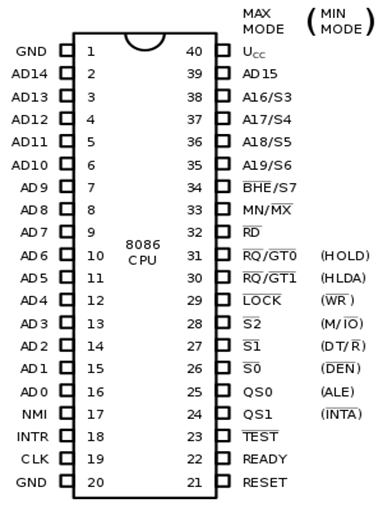
The description of the pins of 8086 is as follows: AD0-AD15 (Address Data Bus): Bidirectional address/data lines. These are low order address bus. They are multiplexed with data. When these lines are used to transmit memory address, the symbol A is used instead of AD, for example, A0- A15. A16 - A19 (Output): High order address lines. These are multiplexed with status signals. A16/S3, A17/S4: A16 and A17 are multiplexed with segment identifier signals S3 and S4. A18/S5: A18 is multiplexed with interrupt status S5. A19/S6: A19 is multiplexed with status signal S6. BHE/S7 (Output): Bus High Enable/Status. During T1, it is low. It enables the data onto the most significant half of data bus, D8-D15. 8-bit device connected to upper half of the data bus use BHE signal. It is multiplexed with status signal S7. S7 signal is available during T3 and T4. RD (Read): For read operation. It is an output signal. It is active when LOW. Ready (Input): The addressed memory or I/O sends acknowledgment through this pin. When HIGH, it denotes that the peripheral is ready to transfer data. RESET (Input): System reset. The signal is active HIGH. CLK (input): Clock 5, 8 or 10 MHz. INTR: Interrupt Request. NMI (Input): Non-maskable interrupt request. TEST (Input): Wait for test control. When LOW the microprocessor continues execution otherwise waits. VCC: Power supply +5V dc. GND: Ground. Operating Modes of 8086There are two operating modes of operation for Intel 8086, namely the minimum mode and the maximum mode. When only one 8086 CPU is to be used in a microprocessor system, the 8086 is used in the Minimum mode of operation. In a multiprocessor system 8086 operates in the Maximum mode. Pin Description for Minimum ModeIn this minimum mode of operation, the pin MN/MX is connected to 5V D.C. supply i.e. MN/MX = VCC. The description about the pins from 24 to 31 for the minimum mode is as follows: INTA (Output): Pin number 24 interrupts acknowledgement. On receiving interrupt signal, the processor issues an interrupt acknowledgment signal. It is active LOW. ALE (Output): Pin no. 25. Address latch enable. It goes HIGH during T1. The microprocessor 8086 sends this signal to latch the address into the Intel 8282/8283 latch. DEN (Output): Pin no. 26. Data Enable. When Intel 8287/8286 octal bus transceiver is used this signal. It is active LOW. DT/R (output): Pin No. 27 data Transmit/Receives. When Intel 8287/8286 octal bus transceiver is used this signal controls the direction of data flow through the transceiver. When it is HIGH, data is sent out. When it is LOW, data is received. M/IO (Output): Pin no. 28, Memory or I/O access. When this signal is HIGH, the CPU wants to access memory. When this signal is LOW, the CPU wants to access I/O device. WR (Output): Pin no. 29, Write. When this signal is LOW, the CPU performs memory or I/O write operation. HLDA (Output): Pin no. 30, Hold Acknowledgment. It is sent by the processor when it receives HOLD signal. It is active HIGH signal. When HOLD is removed HLDA goes LOW. HOLD (Input): Pin no. 31, Hold. When another device in microcomputer system wants to use the address and data bus, it sends HOLD request to CPU through this pin. It is an active HIGH signal. Pin Description for Maximum ModeIn the maximum mode of operation, the pin MN/�MX is made LOW. It is grounded. The description about the pins from 24 to 31 is as follows: QS1, QS0 (Output): Pin numbers 24, 25, Instruction Queue Status. Logics are given below:
S0, S1, S2 (Output): Pin numbers 26, 27, 28 Status Signals. These signals are connected to the bus controller of Intel 8288. This bus controller generates memory and I/O access control signals. Logics for status signal are given below:
LOCK (Output): Pin no. 29. It is an active LOW signal. When this signal is LOW, all interrupts are masked and no HOLD request is granted. In a multiprocessor system all other processors are informed through this signal that they should not ask the CPU for relinquishing the bus control. RG/GT1, RQ/GT0 (Bidirectional): Pin numbers 30, 31, Local Bus Priority Control. Other processors ask the CPU by these lines to release the local bus. In the maximum mode of operation signals WR, ALE, DEN, DT/R etc. are not available directly from the processor. These signals are available from the controller 8288. Functional units of 80868086 contains two independent functional units: a Bus Interface Unit (BIU) and an Execution Unit (EU). 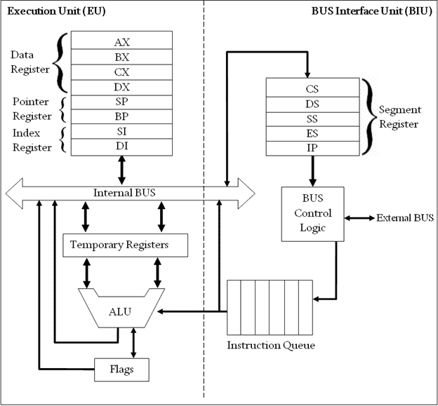
Fig: Block Diagram of Intel 8086 Microprocessor (8086 Architecture) Bus Interface Unit (BIU)The segment registers, instruction pointer and 6-byte instruction queue are associated with the bus interface unit (BIU). The BIU:
It has the following functional parts:
Execution Unit (EU)
InterruptsInterrupt is a process of creating a temporary halt during program execution and allows peripheral devices to access the microprocessor. Microprocessor responds to these interrupts with an interrupt service routine (ISR), which is a short program or subroutine to instruct the microprocessor on how to handle the interrupt. There are different types of interrupt in 8086: 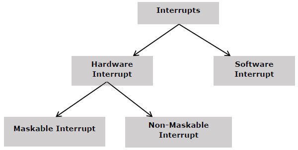
Hardware InterruptsHardware interrupts are that type of interrupt which are caused by any peripheral device by sending a signal through a specified pin to the microprocessor. The Intel 8086 has two hardware interrupt pins:
NMI: NMI is a single Non-Maskable Interrupt having higher priority than the maskable interrupt.
INTR: The INTR is a maskable interrupt. It can be enabled/disabled using interrupt flag (IF). After receiving INTR from external device, the 8086 acknowledges through INTA signal. It executes two consecutive interrupt acknowledge bus cycles. Software InterruptA microprocessor can also be interrupted by internal abnormal conditions such as overflow; division by zero; etc. A programmer can also interrupt microprocessor by inserting INT instruction at the desired point in the program while debugging a program. Such an interrupt is called a software interrupt. The interrupt caused by an internal abnormal conditions also came under the heading of software interrupt. Example of software interrupts are:
Interrupt pointer table for 8086 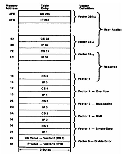
Fig: Interrupt pointer table for 8086 The 8086 can handle up to 256, hardware and software interrupts. 1KB memory acts as a table to contain interrupt vectors (or interrupt pointers), and it is called interrupt vector table or interrupt pointer table. The 256 interrupt pointers have been numbered from 0 to 255 (FF hex). The number assigned to an interrupt pointer is known as type of that interrupt. For example, Type 0, Type 1, Type 2,...........Type 255 interrupt. Addressing modes of 8086The way for which an operand is specified for an instruction in the accumulator, in a general purpose register or in memory location, is called addressing mode. The 8086 microprocessors have 8 addressing modes. Two addressing modes have been provided for instructions which operate on register or immediate data. These two addressing modes are: Register Addressing: In register addressing, the operand is placed in one of the 16-bit or 8-bit general purpose registers. Example
Immediate Addressing: In immediate addressing, the operand is specified in the instruction itself. Example
The remaining 6 addressing modes specify the location of an operand which is placed in a memory. These 6 addressing modes are: Direct Addressing: In direct addressing mode, the operand?s offset is given in the instruction as an 8-bit or 16-bit displacement element. Example
The instruction adds the content of the offset address 0301 to AL. the operand is placed at the given offset (0301) within the data segment DS. Register Indirect Addressing: The operand's offset is placed in any one of the registers BX, BP, SI or DI as specified in the instruction. Example
It moves the contents of memory locations addressed by the register BX to the register AX. Based Addressing: The operand's offset is the sum of an 8-bit or 16-bit displacement and the contents of the base register BX or BP. BX is used as base register for data segment, and the BP is used as a base register for stack segment. Effective address (Offset) = [BX + 8-bit or 16-bit displacement]. Example
Indexed Addressing: The offset of an operand is the sum of the content of an index register SI or DI and an 8-bit or 16-bit displacement. Offset (Effective Address) = [SI or DI + 8-bit or 16-bit displacement] Example
Based Indexed Addressing: The offset of operand is the sum of the content of a base register BX or BP and an index register SI or DI. Effective Address (Offset) = [BX or BP] + [SI or DI] Here, BX is used for a base register for data segment, and BP is used as a base register for stack segment. Example
Based Indexed with Displacement: In this mode of addressing, the operand's offset is given by: Effective Address (Offset) = [BX or BP] + [SI or DI] + 8-bit or 16-bit displacement Example
Next TopicInstruction Set of 8086
|
 For Videos Join Our Youtube Channel: Join Now
Feedback
- Send your Feedback to [email protected]
Help Others, Please Share


