| |

Memory and I/O InterfacingSeveral memory chips and I/O devices are connected to a microprocessor. The following figure shows a schematic diagram to interface memory chips and I/O devices to a microprocessor. 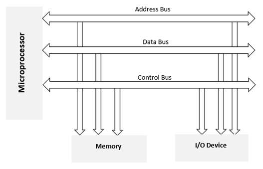
Memory InterfacingWhen we are executing any instruction, the address of memory location or an I/O device is sent out by the microprocessor. The corresponding memory chip or I/O device is selected by a decoding circuit. Memory requires some signals to read from and write to registers and microprocessor transmits some signals for reading or writing data. The interfacing process includes matching the memory requirements with the microprocessor signals. Therefore, the interfacing circuit should be designed in such a way that it matches the memory signal requirements with the microprocessor's signals. I/O interfacingAs we know, keyboard and displays are used as communication channel with outside world. Therefore, it is necessary that we interface keyboard and displays with the microprocessor. This is called I/O interfacing. For this type of interfacing, we use latches and buffers for interfacing the keyboards and displays with the microprocessor. But the main drawback of this interfacing is that the microprocessor can perform only one function. 8279 Programmable KeyboardThe Intel 8279 is a programmable keyboard interfacing device. Data input and display are the integral part of microprocessor kits and microprocessor-based systems. 8279 has been designed for the purpose of 8-bit Intel microprocessors. 8279 has two sections namely keyboard section and display section. The function of the keyboard section is to interface the keyboard which is used as input device for the microprocessor. It can also interface toggle or thumb switches. The purpose of the display section is to drive alphanumeric displays or indicator lights. It is directly connected to the microprocessor bus. The microprocessor is relieved from the burden of scanning the keyboard or refreshing the display. Some important Features are:
8257 DMA ControllerThe data transfer from fast I/O devices to the memory or from the memory to I/O devices through the accumulator is a time consuming process. For this situation, the Direct Memory Access (DMA) technique is preferred. In DMA data transfer scheme, data is directly transferred from an I/O device to RAM or from RAM to an I/O device. Using a DMA controller, the device requests the CPU to hold its address, data and control bus, so the device is free to transfer data directly to/from the memory. The DMA data transfer is initiated only after receiving HLDA signal from the CPU. How DMA operations are performed?Following are the operations performed by a DMA:
Intel 8257
8257 ArchitectureThe following diagram is the architecture of Intel 8257: 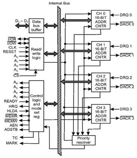
8257 Pin Description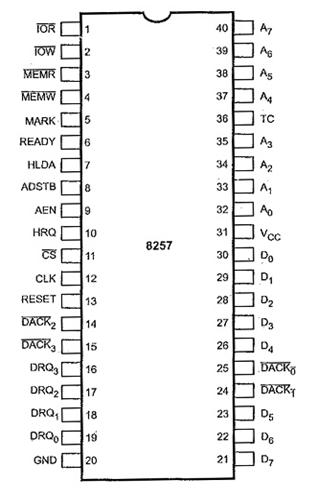
DRQ0 - DRQ3: These are DMA request lines. An I/O device sends the DMA request on one of these lines. On the line, a HIGH status generates a DMA request. DACK0 - DACK3: These are DMA acknowledge lines. The Intel 8257 sends an acknowledge signal through one of these lines informing an I/O device that it has been selected for DMA data transfer. On the line, a LOW acknowledges the I/O device. A0 - A7: These are address lines. A0 - A3 are bidirectional lines. These lines carry 4 LSBs of 16-bit memory address generated by the 8257 in the master mode. In the slave mode, these lines are all the input lines. The inputs select one from the registers to be read or programmed. A4 - A7 lines gives tristated outputs in the master mode which carry 4 through 7 of the 16-bit memory address generated by the Intel 8257. D0 - D7: These are data lines. These are bidirectional three state lines. While programming the controller the CPU sends data for the DMA address register, the byte count register and the mode set register through these data lines. AEN: Address latch enable. ADSTB: A HIGH on this line latches the 8MSBs of the address, which are sent on D-bus, into Intel 8212 connected for this purpose. CS: It is chip select. (I/OR): I/O read. It is a bidirectional line. In output mode it is used to access data from the I/O device during the DMA write cycle. (I/OW): I/O write. It is a bidirectional line. In output mode it allows the transfer of data to the I/O device during the DMA read cycle. Data is transferred from the memory. MEMR: Memory read MEMW: Memory write TC: Byte count (Terminal count). MARK: Modulo 128 Mark. CLK: Clock HRQ: Hold request HLDA: Hold acknowledge
Next TopicMicrocontroller
|
 For Videos Join Our Youtube Channel: Join Now
Feedback
- Send your Feedback to [email protected]
Help Others, Please Share


