| |

Peripheral DevicesTo communicate with the outside world microcomputers use peripherals (I/O devices). Commonly used peripherals are: A/D converter, D/A converter, CRT, printers, Hard disks, floppy disks, magnetic tapes etc. Peripherals are connected to the microcomputer through electronic circuits known as interfacing circuits. Programmable Peripheral interface (PPI)A programmable peripheral interface is a multiport device. The ports may be programmed in a variety of ways as required by the programmer. The device is very useful for interfacing peripheral devices. The term PIA, Peripheral Interface Adapter is also used by some manufacturer. Intel 8255The Intel 8255 is a programmable peripheral interface (PPI). It has two versions, namely the Intel 8255A and Intel 8255A-5. General descriptions for both are same. There are some differences in their electrical characteristics. Hereafter, they will be referred to as 8255. Its main functions are to interface peripheral devices to the microcomputer. It has three 8-bit ports, namely Port A, Port B and Port C. The port C has been further divided into two 4-bit ports, port C upper and Port C lower. Thus a total of 4-ports are available, two 8-bit ports and two 4-bit ports. Each port can be programmed either as an input port or an output port. Operating Modes of 8255The Intel 8255 has the following three modes of operation which are selected by software: Mode 0 - Simple Input/output: The 8255 has two 8-bit ports (Port A and Port B) and two 4-bit ports (Port Cupper and Port Clower). In Mode 0 operation, a port can be operated as a simple input or output port. Each of the 4 ports of 8255 can be programmed to be either an input or output port. Mode 1-Strobed Input/output: Mode 1 is strobed input/output mode of operation. The Port A and Port B both are designed to operate in this mode of operation. When Port A and Port B are programmed in Mode 1, six pins of Port C are used for their control. Mode 2 -Bidirectional Port: Mode 2 is strobed bidirectional mode of operation. In this mode Port A can be programmed to operate as a bidirectional port. The mode 2 operation is only for Port A. When Port A is programmed in Mode 2, the port B can be used either Mode 1 or Mode 0. Architecture of Intel 8255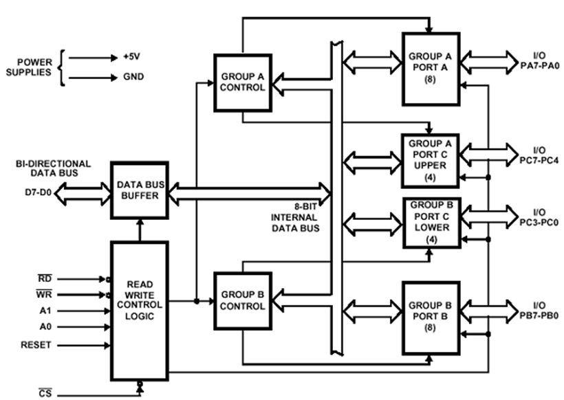
Intel 8255A pin descriptionIt is a 40 pin I.C. package. It operates on a single 5 Vd.c. supply. Its important characteristics are as follows:
Ambient temperature 0 to 700C,
Voltage on any pin: 0.5 V to 7 V.
Power dissipation 1 Watt
VIL = Input low voltage = Minimum 0.5 V, Maximum 0.8 V.
VIH = Input high voltage = Minimum 2 V, Maximum Vcc.
VOL = Output low voltage = 0.45 V
VOH = Output High Voltage = 2.4 V
IDR = Darlington drive connect = Minimum 1 mA, Maximum 4 mA of any 8 pins of the port.
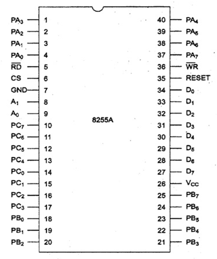
The pins of various ports are as follows:
PA0 - PA7 8 Pins of port A
PB0 - PB7 8 pins of port B
PC0 - PC3 4 pins of port Clower
PC4 - PC7 4 pins of Port Cupper
The important control signals are: CS (Chip Select): It is a chip select signal. The LOW status of this signal enables communication between the CPU and 8255. RD (READ): When RD goes LOW the 8255 sends out data or status information to the CPU on the data bus. In other words it allows the CPU to read data from the input port of 8255. WR (Write): When WR goes LOW the CPU writes data or control word into 8255. The CPU writes data into the output port of 8255 and the control word into the control word register. RESET: RESET is an active high signal. It clears the control register and sets all ports in the input mode. A0 and A1: The selection of input port and control word register is done using A0 and A1 in conjunction with RD and WR. A0 and A1 are normally connected to the least significant bits of the address bus. If two 8255 units are used the addresses of ports are as follows: For the First unit of 8255, i.e. 8255.1:
For the 2nd unit of 8255, i.e. 8255.2:
8253 Programmable Interval TimerA programmable counter/interval timer is used in real time application for timing and counting function such as BCD/binary counting, generation of accurate time delay, generation of square wave of desired frequency, rate generation, hardware/software triggered strobe signal, one shot signal of desired width etc. Popular programmable interval timer chips are Intel 8253 and 8254. Both are pin to pin compatible and operate in the following six modes: Mode 0: Interrupt on terminal count Mode 1: Programmable one-shot Mode 2: Rate generator Mode 3: Square wave generator Mode 4: Software triggered mode Mode 5: Hardware triggered mode The 8254 is compatible to 8086, 8088, 8085 and most other microprocessors. The 8253 is compatible to 8085 microprocessor. The 8254 is superset of the 8253. Architecture of Intel 8253/54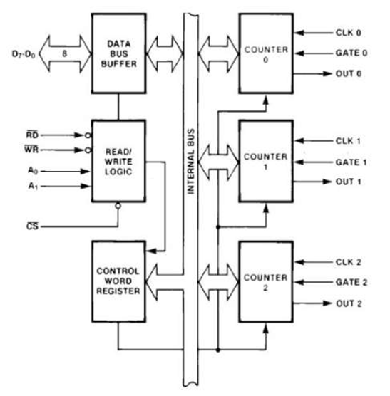
Intel 8253The 8253 is 24-pin IC and operates at 5 Vd.c.. It contains three independent 16-bit counters. The programmer can program 8253 to operate in any one of the 6 operating modes. It operates under software control. The description of its important pins is as follows: 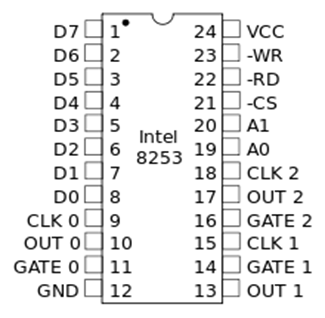
RD (Read): When this pin is LOW the CPU reads data. �WR: (Write): When this is low, the CPU outputs data in the form of mode information or loading of counters. A0, A1: These pins are connected to the address bus. These are used to select one of three counters. These are also used to address the control word registers for mode selection. CS: Chip Select. D0 - D7: Bidirectional data bus. CLK0, CLK1 and CLK2 are clock for Counter 0, Counter 1 and Counter 2 respectively. GATE0, GATE1 and GATE2 are gate terminals of Counter 0, Counter 1 and Counter 2 respectively. OUT0, OUT1 and OUT2 are output terminals of Counter 0, Counter 1 and Counter 2 respectively. The 8253 contains a data buffer, read/write logic and control word register as described below: Data Bus Buffer: This buffer is within 8253. It is a 3-state, bidirectional, 8-bit buffer. It is used to interface 8253 to the system data bus through D0 - D7 lines. Read/Write logic: The 8253 contains a read/write logic which accepts input from the system bus and then generates control signals for the operation of 8253. The following table shows the status of pins associated with read/write logic for various controls:
Note: - X indicates undefined state. It means that it does not matter whether the state is 0 or 1.Counter Word Register: When the pins A0, A1 are 11, the control word register is selected. The control word format is shown below: D7 D6 D5 D4 D3 D2 D1 D0
The bits D7 and D6 of the control word are to select one of the 3 counters. D5 and D4 are for loading/reading the count. D3, D2 and D1 are for the selection of operating mode of the selected counter. These are six modes of operation for each counter of 8253. The six modes of operation are: MODE 0, MODE 1, MODE 2, MODE 3, MODE 4 and MODE 5. The bit D0 is for the selection of binary or BCD counting. 8253/54 Operational Modes8253/54 can be operated in 6 different modes. These modes are: MODE 0 : Interrupt on Terminal Count
MODE 1 : Programmable One-Shot
MODE 2 : RATE Generator
MODE 3 : Square Wave Generation
MODE 4 : Software Triggered Strobe
MODE 5 : Hardware Triggered Strobe
Next Topic#
|
 For Videos Join Our Youtube Channel: Join Now
Feedback
- Send your Feedback to [email protected]
Help Others, Please Share


