Microprocessor Architecture
The microprocessor is the CPU (Central Processing Unit) of a computer. It is the heart of the computer. Here, we will describe Intel 8085 as it is one of the most popular 8-bit microprocessor.
Intel 8085
Intel 8085 is an 8-bit, NMOS microprocessor designed by Intel in 1977.
It has following configuration:
- It is a 40 pin I.C. package fabricated on a single LSI chip.
- The Intel 8085 uses a single +5Vd.c. supply for its operation.
- Intel 8085?s clock speed is about 3 MHz; the clock cycle is of 320ns.
- 8 ?bit data bus.
- Address bus is of 16-bit, which can address up to 64KB
- 16-bit stack pointer
- 16 bit PC (Program Counter)
- Six 8-bit registers are arranged in pairs :BC, DE, HL
Intel 8085 is used in mobile phones, microwave ovens, washing machines etc.
The below diagram shows the block diagram of Intel 8085:

ALU
The Arithmetic and Logic Unit, ALU performs the arithmetic and logical operations:
- Addition
- Subtraction
- Logical AND
- Logical OR
- Logical EXCLUSIVE OR
- Complement (Logical NOT)
- Increment (add 1)
- Decrement (subtract 1)
- Left shift, Rotate left, Rotate right
- Clear, etc.
Timing and Control Unit
The timing and control unit is the section of the CPU.
- It is used to generate timing and control signals which are necessary for the execution of instructions.
- It is used to control data flow between CPU and peripherals (including memory).
- It is used to provide status, control and timing signals which are required for the operation of memory and I/O devices.
- It is used to control the entire operations of the microprocessor and peripherals connected to it.
Thus we can see that the control unit of the CPU acts as the brain of the computer system.
Registers
Registers are used for temporary storage and manipulation of data and instructions by the microprocessor. Data remain in the registers till they are sent to the I/O devices or memory. Intel 8085 microprocessor has the following registers:
- One 8-bit accumulator (ACC) i.e. register A
- Six general purpose registers of 8-bit, these are B,C, D, E, H and L
- One 16-bit stack pointer, SP
- One 16-bit Program Counter, PC
- Instruction register
- Temporary register
In addition to the above mentioned registers the 8085 microprocessor contains a set of five flip-flops which serve as flags (or status flags).
A flag is a flip-flop which indicates some conditions which arises after the execution of an arithmetic or logical instruction.
- Accumulator (ACC): The accumulator is an 8-bit register associated with the ALU. The register 'A' is an accumulator in the 8085. It is used to hold one of the operands of an arithmetic and logical operation.
The final result of an arithmetic or logical operation is also placed in the accumulator.
- General-Purpose Registers: The 8085 microprocessor contains six 8-bit general purpose registers. They are: B, D, C, E, H and L register.
To hold data of 16-bit a combination of two 8-bit registers can be employed.
The combination of two 8-bit registers is called register pair. The valid register pairs in the 8085 are: D-E, B-C and H-L. The H-L pair is used to act as a memory pointer.
- Program Counter (PC): It is a 16-bit special purpose register. It is used to hold the address of memory of the next instruction to be executed. It keeps the track of the instruction in a program while they are being executed.
The microprocessor increments the content of the next program counter during the execution of an instruction so that at the end of the execution of an instruction it points to the next instruction?s address in the program.
- Stack Pointer (SP): It is a 16-bit special function register used as memory pointer. A stack is nothing but a portion of RAM. In the stack, the contents of only those registers are saved, which are needed in the later part of the program.
The stack pointer (SP) controls the addressing of the stack. The Stack Pointer contains the address of the top element of data stored in the stack.
- Instruction Register: The instruction register holds the opcode (operation code or instruction code) of the instruction which is being decoded and executed.
- Temporary Register: It is an 8-bit register associated with the ALU. It holds data during an arithmetic/logical operation. It is used by the microprocessor. It is not accessible to programmer.
- Flags: The Intel 8085 microprocessor contains five flip-flops to serve as a status flags. The flip-flops are reset or set according to the conditions which arise during an arithmetic or logical operation.
The five status flags of Intel 8085 are:
- Carry Flag (CS)
- Parity Flag (P)
- Auxiliary Carry Flag (AC)
- Zero Flag(Z)
- Sign Flag(S)
If a flip-flop for a particular flag is set, then it indicates 1. When it is reset, it indicates 0.
Data and Address Bus
- The Intel 8085 is an 8-bit microprocessor. Its data bus is 8-bit wide and therefore, 8 bits of data can be transmitted in parallel from or to the microprocessor.
- The Intel 8085 requires an address bus of 16-bit wide as the memory addresses are of 16-bits.
- The 8 most significant bits of the address are transmitted by the address bus, A-bus (pins A8 ? A15).
- The 8 least significant bits of the address are transmitted by data/address bus, AD-bus (pins AD0 ? AD7).
Pin Configuration
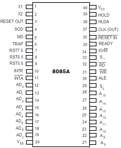
Fig: Pin diagram of Intel 8085 microprocessor
The descriptions of various pins are as follows:
Address Bus and Data Bus
- A8 ? A15 (Output): These are address bus and are used for the most significant bits of the memory address or 8-bits of I/O address.
- AD0 ? AD7 (Input/output): These are time multiplexed address/data bus i.e. they serve dual purpose. They are used for the least significant 8 bits of the memory address or I/O address during the first cycle. Again they are used for data during 2nd and 3rd clock cycles.
Control and Status Signals
- ALE (Output): ALE stands for Address Latch Enable signal. ALE goes high during first clock cycle of a machine cycle and enables the lower 8-bits of the address to be latched either into the memory or external latch.
- IO/M (Output): It is a status signal which distinguishes whether the address is for memory or I/O device.
- S0, S1 (Output): These are status signals sent by the microprocessors to distinguish the various types of operation given in table below:
Status codes for Intel 8085
| S1 |
S0 |
Operations |
| 0 |
0 |
HALT |
| 0 |
1 |
WRITE |
| 1 |
0 |
READ |
| 1 |
1 |
FETCH |
- RD (Output): RD is a signal to control READ operation. When it goes low, the selected I/O device or memory is read.
- WR (Output): WR is a signal to control WRITE operation. When it goes low, the data bus' data is written into the selected memory or I/O location.
- READY (Input): It is used by the microprocessor to sense whether a peripheral is ready to transfer a data or not. If READY is high, the peripheral is ready. If it is low the micro processor waits till it goes high.
Interrupts and Externally Initiated Signals
- HOLD (INPUT): HOLD indicates that another device is requesting for the use of the address and data bus.
- HLDA (OUTPUT): HLDA is a signal for HOLD acknowledgement which indicates that the HOLD request has been received. After the removal of this request the HLDA goes low.
- INTR (Input): INTR is an Interrupt Request Signal. Among interrupts it has the lowest priority. The INTR is enabled or disabled by software.
- INTA (Output): INTA is an interrupt acknowledgement sent by the microprocessor after INTR is received.
- RST 5.5, 6.5, 7.5 and TRAP (Inputs): These all are interrupts. When any interrupt is recognized the next instruction is executed from a fixed location in the memory as given below:
| Line |
Location from which next instruction is picked up |
| TRAP |
0024 |
| RST 5.5 |
002C |
| RST 6.5 |
0034 |
| RST 7.5 |
003C |
RST 7.5, RST 6.5 and RST 5.5 are the restart interrupts which cause an internal restart to be automatically inserted.
The TRAP has the highest priority among interrupts. The order of priority of interrupts is as follows:
- TRAP (Highest priority)
- RST 7.5
- RST 6.5
- RST 5.5
- INTR (Lowest priority).
Reset Signals
- RESET IN (Input): It resets the program counter (PC) to 0. It also resets interrupt enable and HLDA flip-flops. The CPU is held in reset condition till RESET is not applied.
- RESET OUT (Output): RESET OUT indicates that the CPU is being reset.
Clock Signals
- X1, X2 (Input): X1 and X2 are terminals to be connected to an external crystal oscillator which drives an internal circuitry of the microprocessor. It is used to produce a suitable clock for the operation of microprocessor.
- CLK (Output): CLK is a clock output for user, which can be used for other digital ICs. Its frequency is same at which processor operates.
Serial I/O Signals
- SID (Input): SID is data line for serial input. The data on this line is loaded into the seventh bit of the accumulator when RIM instruction is executed.
- SOD (Output): SOD is a data line for serial output. The seventh bit of the accumulator is output on SOD line when SIM instruction is executed.
Power Supply
Vcc : +5 Vlots supply
Vss : ground reference
8085 Instructions
An instruction of computer is a command given to the computer to perform a specified operation on given data. Some instructions of Intel 8085 microprocessor are: MOV, MVI, LDA, STA, ADD, SUB, RAL, INR, MVI, etc.
Opcode and Operands
Each instruction contains two parts: Opcode (Operation code) and Operand.
The 1st part of an instruction which specifies the task to be performed by the computer is called Opcode.
The 2nd part of the instruction is the data to be operated on, and it is called Operand. The Operand (or data) given in the instruction may be in various forms such as 8-bit or 16-bit data, 8-bit or 16-bit address, internal registers or a register or memory location.
Instruction Word Size
A digital computer understands instruction written in binary codes (machine codes). The binary codes of all instructions are not of the same length.
According to the word size, the Intel 8085 instructions are classified into the following three types:
- One byte instruction
- Two byte instruction
- Three byte instruction
1. One-byte instruction: Examples of one byte instructions are:
- MOV A, B - Move the content of the register B to register A.
- ADD B ? Add the content of register B to the content of the accumulator.
All the above two examples are only one byte long. All one-byte instructions contain information regarding operands in the opcode itself.
2. Two-byte instruction: In a two byte instruction the first byte of the instruction is its opcode and the second byte is either data or address.
Example:
MVI B, 05; 05 moved to register B.
06, 05; MVI B, 05 is in the code form.
The first byte 06 is the opcode for MVI B and second byte 05 is the data which is to be moved to register B.
3. Three-byte instruction: The first byte of the instruction is its opcode and the second and third bytes are either 16-bit data or 16-bit address.
Example:
LXI H, 2400H; Load H-L Pair with 2400H
21, 00, 24; LXI H, 2400H in the code form
The first byte 21 is the opcode for the instruction LXI H. The second 00 is 8 LSBs of the data (2400H), which is loaded into register L. The third byte 24 is 8 MSBs of the data (2400H), which is loaded into register H.
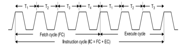
Instruction Cycle
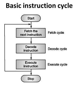
The time required to fetch an instruction and necessary data from memory and to execute it, is called an instruction cycle. Or the total time required to execute an instruction is given by:
Where,
IC = Instruction Cycle
FC = Fetch Cycle
EC = Execute Cycle
Timing Diagram for Instruction Cycle
- Fetch the instruction (Fetch Cycle)
In the beginning of the fetch cycle, the content of the program counter (PC), which is the address of the memory location where opcode is available, is sent to the memory. The memory puts the opcode on the data bus so as to transfer it to the CPU.
The whole operation of fetching an opcode takes three clock cycles. A slow memory may take more time.
- Decode the instruction (Decode Cycle)
The opcode fetched from the memory goes to the data register, DR and then to instruction register, IR. From the IR it goes to the decoder circuitry which decodes the instruction. Decoder circuitry is within the microprocessor.
- Execute the Instruction (Execute Cycle)
After the instruction is decoded, execution begins.
If the operand is reside the general purpose registers, execution is immediately performed. The time taken in decoding and execution of an instruction is one clock cycle.
In some situations, an execute cycle may involve one or more read or write cycles or both.
Read Cycle: If an instruction contains data or operand address which are in the memory, the CPU has to perform some read operations to get the desired data. In case of a read cycle the instruction received from the memory are data or operand address instead of an opcode.
Write Cycle: In write cycle data are sent from the CPU to the memory or an output device.
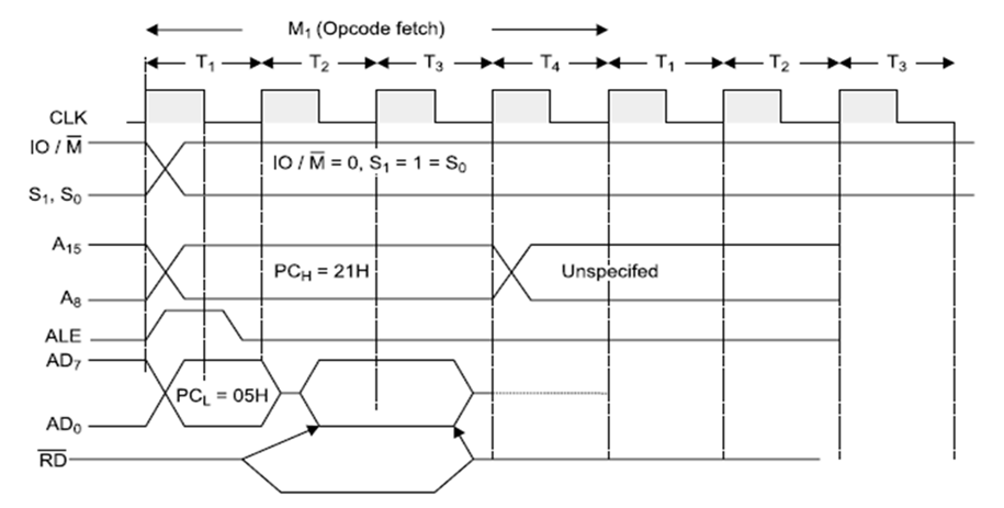
The necessary steps carried out to perform the operation of accessing either memory or input output device, constitute a machine cycle. In other words, necessary steps carried out to perform a fetch, a read or a write operation constitutes a machine cycle.
One sub-division of an operation performed in one clock cycle is called a state or T-state. In short, one clock cycle of the system clock is referred to as a state.
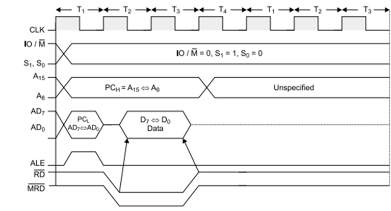
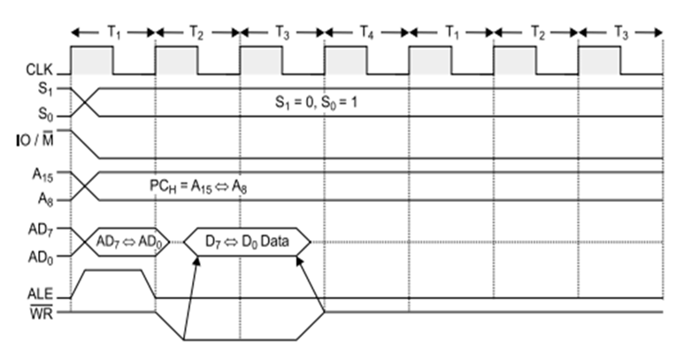
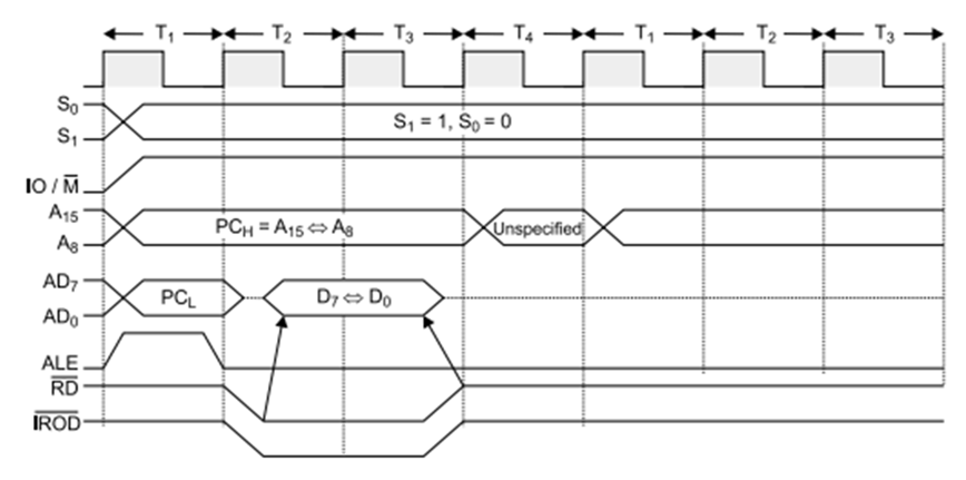
Timing Diagram
The necessary steps carried out in a machine cycle can be represented graphically. Such a graphical representation is called timing diagram. The timing diagram for opcode fetch, memory read, memory write, I/O read and I/O write will be discussed below:
- Timing Diagram for Opcode Fetch Cycle:
- Timing Diagram for Memory Read
- Timing Diagram for Memory Write
- Timing Diagram for I/O Read
- Timing Diagram for I/O Write
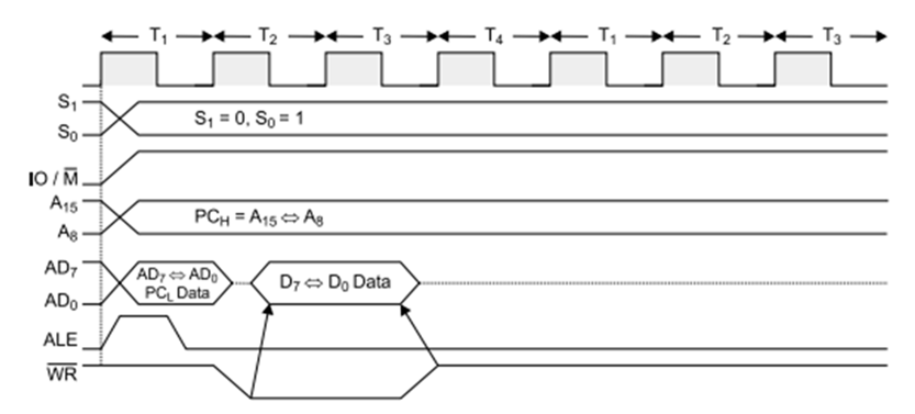
In the above diagrams, the basic used parameters are:
ALE: ALE indicates the availability of a valid address on the multiplexed address/data lines. When it is high or 1, then it acts as an address bus and when low or 0, then it acts as a data bus.
RD (low active): If it is high or 1, then no data is read by the microprocessor. If signal is low or 0, then data is read by the microprocessor.
WR (low active): If it is high or 1, then no data is written by the microprocessor. If signal is low or 0, then data is written by the microprocessor.
IO/M (low active): A high or 1 on this signal indicates I/O operation while a low or 0 indicates memory operation.
S0, S1: S0 and S1 Indicate the type of machine cycle in progress.
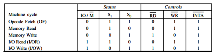
The below table, shows the status of different control signal for different operation:
| 
 For Videos Join Our Youtube Channel: Join Now


