| |

Digital Electronics MCQs1) Which number system has a base 16
Answer: a Explanation: Hexadecimal is a number system with a base 16. We can divide the word HEXA+DECIMAL for better understanding; it means 6 and 10 make 16. It is the easiest way to write and count numbers represented in terms of base 16. There are sixteen distinct digits in the hexadecimal system, it starts from 0, 1,2,3,4,5,6,7,8,9, A, B, C, D, E and end to F. Where A= 10, B=11, C=12, D=13, E=14, F=15. It is usually represented by 4 bits in binary number system by 8421 code. 2) What is a digital-to-analog converter?
Answer: d Explanation: A "digital-to-analog converter" or DAC refers to an electronic device that converts the digital signals (discrete-time signal) to an analog signal (Continuous-time signal). In other words, we can say that an electronic device converts the signal of 0 and 1 (Binary) into the analog form. For example, the amplitude of the output signal varies according to the input values. 3) The following hexadecimal number (1E.43)16 is equivalent to
Answer: b Explanation: If you want to convert a hexadecimal number into an octal number, the first thing you need to do is convert a hexadecimal number into binary form by writing the binary equivalent of each digit in the form of 4 bits. Once you write the number into binary form, you need to group the binary equivalent in 3 bits, then for each of the three bits, the respective digit is written. (1E.43)16 = (0001 1110.0100 0011)2 = (00011110.01000011)2 = (011110.010000110)2 = (011 110.010 000 110)2 = (36.206)8 4) How many entries will be in the truth table of a 4-input NAND gate?
Answer: d Explanation: A NAND gate is a universal logic gate that performs the negation (NOT) of an AND logic operations in digital circuits. As we know, Y = 2n Y number of Entries in the truth table Where, n = number of inputs. 5) How many bits are needed to store one BCD digit?
Answer: b Explanation: BCD stands for Binary Coded Decimal. It is a type of binary encoding where each decimal digit is represented by a fixed number of bits, usually 4. It is also called 8421 code to represent the maximum number 15. BCD can encode only from 0-9. For example, Decimal number 456, its equivalent BCD code is 0100 0101 0110 6) Convert (312)8 into decimal
Answer: b Explanation: Octal to decimal conversion is usually obtained by multiplying 8 to the power of base along with the value at the index position. (312)8 = 3 * 82 + 1* 81 + 2* 80 = 192 + 8 +2 = (202)10 7) A SCR (Silicon Controlled Rectifier) is a
Answer: b Explanation: SCR stands for Silicon Controlled Rectifier; it is a family of thyristors with the same property as thyristors. It is a semiconductor device with three junctions. They are of two types: npnp and pnpn. For the pnpn type, the inner player has a gate terminal, the outer player has an anode terminal, and the outer n layer has a cathode terminal. The SCR controls the flow of anode current once the gate is triggered. 8) Which semiconductor device is not a current triggering device?
Answer: b Explanation: MOSFET stands for Metal Oxide Semiconductor Field Effects Transistor. It is a semiconductor device that is extensively used for switching and amplifying the signals in digital devices. The MOSFET is the main part of any integrated circuits, and it can be designed in a single chip because of its small sizes. It is a four-terminal device: source(S), gate(g), drain(d), and body(b). The body(b) is connected to the source, making MOSFETS a three-terminal device like a field-effect transistor. MOSFETS can be used in both digital and Analog circuits, so it is one of the widely used transistors in digital circuits. 9) Which of these sets of logic gates are known as universal gates?
Answer: d Explanation: NAND or NOR gates are used to design all other logic gates, so; they are termed universal gates. 10) What is the addition of the binary number 101001+ 010011=?
Answer: b Explanation: If you want to add any binary number, first, you need to know the binary addition rules. 0 + 1 = 1 1 + 0 = 1 0 + 0 = 0 1 + 1 = 0 (with carry 1) 101001+ 010011 = 111100 11) What is the binary subtraction of 101001 - 010110 =?
Answer: a Explanation: If you want to subtract any binary number, first, you need to know the binary subtraction rules. 1 - 0 = 1 0 - 1 = 1 (With borrow 1) 0 - 0 = 0 1 - 1 = 0 therefore, the subtraction of 101001 - 010110 = 010011 12) What is the binary multiplication of 10100 * 01011 =?
Answer: c Explanation: If you want to multiply any binary number, you need to know the binary multiplication rules. 1 * 0 = 0 0 * 1 = 0 0 * 0 = 0 1 * 1 = 1 therefore, the multiplication of 10100 - 01011 = 011011100 13) Divide the binary number: 111001 � 1101 and find the reminder
Answer: c Explanation: If you want to divide any binary number, you need to know the binary division rule. The binary division is accomplished using the long division rule. Therefore, the remainder of 111001 ÷ 1101 = 0101 14) In the toggle mode, a JK flip-flop has
Answer: b Explanation: Toggling means switching between the two states when output changes to its complement on applying clock signal. For example, suppose you assume the initial output to be X (1 or 0), then after toggling, the output state will be X' (0 or 1, respectively). Both j and k should be 1 for toggle in JK flip flop. 15) A classification of integrated circuits with complexities of 30 to 300 equivalent gates on a single chip is known as?
Answer: d Explanation: The terminologies like MSI, SSI, LSI and VLSI came out from the complexity of the integrated circuit. It means the total number of transistors are fabricated on a single chip. Jack Kilby invented the first integrated circuit in 1959, so, after that, the Integrated circuit has emerged like SSI, LSI, MSI and VLSI. In MSI (Medium Scale Integration) = 30 - 300 gates /chip (counters, multiplexers, registers) In LSI (Large Scale Integration) = 300 - 3000 gates /chip (8-bit processors) In SSI (Small-Scale Integration) = 3 - 30 gates /chip (logic gates, flip flops) In VLSI (Very Large-Scale Integration) = >3000 gates / chip (16 bit and 32- bit processors) 16) The inverter can be classified as
Answer: d Explanation: Inverter refers to an electronic device that converts direct current (DC) to alternating current (AC). It has a wide range of applications for small appliances, TVs, DVD players, computer power supply to large electric power supply like photovoltaic solar cells. Based on the type of the input source, Inverters are divided into two categories.
17) Temperature variation is a/an
Answer: a Explanation: Temperature variation is continuous with respect to time. So, it is an analog quantity. 18) 1's complement of 1011001 is
Answer: c Explanation: If you want to calculate 1's complement of any binary number, you need to reverse its binary bits. All the 0's to 1's and 1's to 0's. Therefore, 1's complement of 1011001 = 0100110 19) 2's complement of 1011011 is
Answer: d Explanation: If you want to calculate 2's complement of any binary number, first you need to calculate 1's complement of that number and then add 1 to it. 2's complement of 1011011 = 0100100 + 1 = 0100101. 20) An overflow is a
Answer: c Explanation: An overflow is a software problem that takes place when the processor cannot respond to the output accurately when it gives an out-of-range result. 21) A digital circuit that can store only one bit is a
Answer: c Explanation: A flip-flop refers to an electronic circuit with two stable states that can be used to store the binary data (1,0). Flip-flop can store only one bit of data, either a logic 1 or 0. This logic state can be represented as the voltage on the flip-flop's output because it can be controlled to hold the logic state, effectively a 1 -bit memory. 22) The excess-3 code for 584 is given by
Answer: a Explanation: If you want to calculate the excess-3 code of any number, you need to add "3" to each digit of the same number. In the above problem, the addition of "3" to each digit gives you a new digit "8," "11," and "7." Hence, according to 8421 rules, the corresponding four-bit binary equivalents are 100010110111 23) In Digital electronics (Boolean algebra), the OR operation is performed by which of the given properties
Answer: d Explanation: In Boolean algebra, the distributive properties are given by the following equation: A + BC = (A+B) (A+C) & A(B+C) = AB+AC In Boolean algebra, the commutative properties are given by the following equation: A+B = B+A & A*B = B*A In Boolean algebra, the distributive properties are given by the following equation: A+(B+C) = (A+B) +C & A*(B*C) = (A*B) *C 24) The queue is also known as
Answer: d Explanation: FIFO stands for First In - First Out. The queue is a type of memory based on FIFO, which means the request which has come first will be dealt with first. For example, the line of a crowd for booking railway tickets. The person who came first will get the ticket first. In the case of a Queue data structure, we call an ordinary queue as a FIFO queue. 25) In three-phase half-wave rectifier, each diode conducts for a duration of
Answer: a Explanation: Mainly, there are two types of 3 phase rectifiers: A half-wave rectifier and a full-wave rectifier. Many industries work on 3 phase power supply instead of a single phase. In three-phase half-wave rectifiers, each diode conducts for a duration of 120 0 because the cycle will be repeated itself, and each thyristor conducts for 1200 duration when the firing angle is less than 300. 26) DeMorgan's Law states that
Answer: b Explanation: DeMorgan's theorems play a vital role in digital electronics. It gives an equivalency between the logic gates. There are two distinct types of DeMorgan's theorems: the first gives the equivalent of the NAND gate, and the other gives the equivalent of the NOR gate. As per the dual property of DeMorgan's theorem (AB)' = A' + B' & (A+B) = A' * B' 27) The logical sum of two or more than two logical products is termed as
Answer: c Explanation: SOP stands for "Sum of products." SOP is a way that a Boolean Algebra formula can be written. For example, the sum of product formula: AB + A'B'. In other words, it is defined as the logical sum of two or more logical product terms. POS refers to the logical product of two or more than two logical sum terms. 28) The Minterms for four variables
Answer: b Explanation: Minterms is given by the following formula Minterm = 2n Therefore, 24= 16 minterms are needed. 29) A K-map (Karnaugh map) is an abstract form of which diagram organized as a squares matrix.
Answer: d Explanation: K- Map, also known as Karnaugh map, refers to a pictorial representation of a truth table. It helps in minimizing variables of any Boolean expression. It is also an abstract form of a Venn diagram arranged as a square of a matrix, where each square represents a minterm or maxterm. 30) Which of the given device used in speed control of a DC motor?
Answer: d Explanation: SCR stands for silicon-controlled rectifiers. SCR is used in speed control DC motor. SCR is controlled by a variable resistor potentiometer. Many Industries use variable speed drives for industrial applications. For example, rolling mills, railway traction, etc. 31) One nibble is equal to how many bits
Answer: a Explanation: In digital electronics, the smallest unit of storage consisting of either 0 or 1 is called a bit. The arrangement of such 4 bits is known as a nibble. The arrangement of such 8 bits is known as a byte. 32) Suppose the output of an XNOR gate is 1. Which of the given input combination is correct?
Answer: d Explanation: An XNOR refers to a digital logic gate with two or more inputs and one output that executes logical equality. The output of an XNOR gate is true either all of its inputs are true, or all of its inputs are false. When one of its inputs is false, and others are true, then the output is false. The output of the XNOR gate is given by the following equation. AB + A'B,' For A = 0 AND B = 0 the output will be 1. 33) In DTL, the logic gating function is performed by
Answer: b Explanation: DTL stands for Diode Transistor Logic, where the diode serves as the Input network, and the switching operation is performed by the transistor. DTL is a predecessor of TTL (Transistor-Transistor Logic). The logic functions can be performed using resistors for biasing, transistors to amplify and diodes to switch and isolate inputs, producing logic levels. 34) Which of the given logic family provide minimum power dissipation
Answer: c Explanation: CMOS stands for Complimentary Metal Oxide Semiconductor, which allows low power consumption and less density because it does not consume power in the OFF state. It is a digital logic that utilizes a pair of complementary field-effect transistors to switch the electric current. When the logic gate is ON, one transistor is in on, whereas the other is in OFF condition. 35) The AND operation is equivalent to
Answer: b Explanation: AND operation is equivalent to Intersection. It means Y = A.B i.e. A AND B = A Intersection B. The output is 1, if and only if all the given inputs are 1. 36) TTL is a class of digital circuits built from
Answer: d Explanation: TTL stands for Transistor-Transistor logic. It is a class of type of digital circuits made up of bipolar junction transistors and resistors. BJT has two types of charge carriers: the first one is the electron and the holes. There are two types of BJTs: NPN and PNP. In TTL, resistors play a very short role, and both logic gating and amplifying functions are carried out by the transistors. 37) Which logic unit is the fastest of all the logic families?
Answer: c Explanation: ECL stands for Emitter Coupled Logic. It is the fastest of all the logic families because of its higher transmission rate. In Emitter Coupled Logic,
In CMOS logic,
In TTL,
38) Positive integers must be represented by
Answer: b Explanation: The negative integers are represented by signed numbers on the extreme left side, whereas the positive integers are represented using unsigned numbers. 39) The Ward- Leonard system is used for controlling the speed of
Answer: d Explanation: The Ward Leonard system was implemented and used to control the speed of DC shunt electric motors. Previously, it was quite convenient to obtain a variety of speeds and reversing for industrial applications. The system consisted of any prime mover, including an AC motor driving a DC shunt generator. The armature of the DC generator was directly connected to the shunt motor's armature to be controlled. The DC motor had its magnetic field continuously excited while that of the DC generator, the magnetic field could be controlled in intensity and direction. As the prime mover rotated, the field of the DC generator was adjusted as required, hence its armature current-controlled, this current would be adjusted in magnitude and direction, and this, being fed to the armature of the DC motor, would create a driving torque as it reacted with the continuously applied motor field. 40) When the PIV rating of a diode is exceeded
Answer: c Explanation: PIV stands for Peak Inverse Voltage. In other words, PIV is defined as the maximum voltage that can apply to a diode in the reverse direction. Applying higher voltage will cause the diode to destroy. Start conducting current in the normally "OFF" direction, which will damage the diode and often do things you don't like to your circuit. The exact details depend on the circuit design. We usually select the PIV larger than the largest normal reverse operating voltage in our circuit. If you are making a full-wave rectifier for 220 Vac, you'd typically select a diode with a 240 or more PIV to give some "head room" and "safety factor" on the diode. The minimum should usually be selected like this: round-up from your designed or simulated reverse voltage to the next higher PIV for a diode family that gives you the current you require. 41) Which insulating layer is used in the fabrication of MOSFET?
Answer: d Explanation: A MOSFET is a field-effect transistor. It depends on the presence of an electric field to control the characteristics of the conductive channel. In the MOSFET, the gate is insulated from the substrate by a layer of silicon dioxide, which is basically glass. The charges accumulate on the gate to create the electric field instead of just having them flow out. So, while silicon is the main constituent of the conductive channel, a thin layer of silicon dioxide is used to insulate the gate. 42) CMOS technology used in?
Answer: d Explanation: CMOS stands for Complimentary Metal Oxide Semiconductor. It is a type of (mostly) digital logic that uses a pair of complementary field-effect transistors to switch electric current. There are some analog CMOS devices; they are a lot less common. CMOS technology is used in many electronic devices like Microprocessor, Ram, Microcontroller, and other logic circuits. When the gate is ON, one transistor is on, and the other is off. When the gate is OFF, the first transistor is off, and the other is ON. 43) The basic building blocks of the arithmetic logic unit in digital computers are known as
Answer: a Explanation: The basic building blocks of the arithmetic unit in digital computers are known as adders. Adder is the Arithmetic mathematical function derived out of Logic gates. So, Adder always plays a major role in understanding Digital Electronics. The simplest but the most powerful application of logic gates is Adder. A full adder is similar to a half adder except that instead of 2 inputs and two outputs, there are now three inputs and two outputs. The inputs are carry-in (Cin), X, and Y. Your outputs remain the same, sum, and carry-out (Cout). A half adder is typically only useful for "single digit" addition. A full adder implements the half Adder to link multiple full adders together to achieve higher orders of addition. Sixteen full adders in the group allow 16- bit addition. 44) The number of inputs in a half adder is?
Answer: b Explanation: The total number of inputs in a half adder is 2. The half adder circuit has two inputs: P and Q, which add two input digits and generate a carry and sum. With the help of half Adder, we can design circuits capable of performing simple addition with the help of logic gates. An EXOR gate has two inputs and carries links to input EXOR gates. The output of the half added is also two, SUM and CARRY. 45) Why is a decoder used in digital electronics?
Answer: b Explanation: Decoder is usually used to convert the coded information (BCD) into a non-coded form. In other words, decoders are defined as an electronic device that is used to convert digital signal to an analog signal. The decoders are used in many communication devices that are used to communicate between two devices. The decoder allows n number of inputs and generates 2n numbers of outputs. For example, if we give two inputs, four by two decoder will produce four outputs. 46) How much input and output needed for demultiplexer?
Answer: b Explanation: A demultiplexer or DEMUX is a device that takes a single input line and routes it to one of several digital output lines. A demultiplexer of 2n outputs has n number of select lines, which are used to choose which output line send the input. A demultiplexer is also known as data distributor. 47) A register can be defined as
Answer: d Explanation: An electronic register refers to a form of memory that uses a group of flip-flops that is suitable for storing binary information, such as a byte (8 bits) of data. Each flip flop is a binary cell suitable for storing individual bits of a binary word. The length of the stored binary information depends on the number of flip-flops that make up the register. The information in a register can be transferred form one flip-flop to another flip-flop. 48) The primary difference between a counter and a register is
Answer: c Explanation: The primary difference between a counter and a register is that register has no specific state sequence except in certain conditions. A counter is a special case of a register while the register has the same clock. generally, the register can only be stored, loaded, or used for the stack or as the program counter. The counter does not need to have the same clock. Advantages of Counter: It is used in frequency dividers, Code generators and Period and sequence generators. Advantages of Register: To Produce Time delay, Simplify Combinational Logic and Convert Serial Data to Parallel Data 49) What is the radix of the octal number system?
Answer: c Explanation: A radix of a number system refers to the number of base digits, including zero, that are used to represent large values. In the binary number system, that would be 2 (0,1). In the octal number system, that would be 8 (0 to 7). In the decimal number system, that would be 10 (0 to 9). In the hexadecimal number system, that would be 16 (0 to 15). 50) Dual slop ADC has the value of R = 1 K? and the value of C is 0.44 nano-farad has charging and discharging time for some specific voltage is nine ns and 3 ns, respectively. If the reference voltage is 4.4 V, what is the peak voltage reached by a triangular wave during the charging process?
Answer: b Explanation: 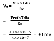
51) The two-transistor model of the SCR is obtained by
Answer: a Explanation: The two- transistor model of the SCR is obtained by bisecting the SCRs top two and bottom two layers. The two-transistor analogy of SCR refers to a method of producing an SCR as a combination of an np-n and a p-np transistor. SCR is a three-terminal device having a p-n-p-n structure. The three terminals of the junctions are the cathode, anode and gate terminal. 52) What is the main function of the filter in a rectifier circuit?
Answer: c Explanation: The main function of the filter in a rectifier circuit is to remove ripples from the rectified output. As we know, rectifiers are primarily used to convert alternating current (AC) to direct current (DC). There we find a considerable AC component in the output, which is called ripple. Many electronic systems require pure direct current supply to drive or power them. To make a efficient continuous power supply that gives pure DC output, we need to remove the AC component from the output of rectifiers. 53) What is the actual meaning of the parallel load of a shift register?
Answer: c Explanation: The actual meaning of the parallel load of a shift register is all flip-flops are present with data. It means that all of the register stages are loaded at a time with new data bits by a single load pulse. In the present condition, the outputs of flip flops will be 1. The value of Preset equals 1 means Q equals 1, this the value of the input is definitely 1. 54) In a 100 kHz clock frequency, 16 bits can be serially entered into a shift register?
Answer: b Explanation: Given f = 100 kHz As we know, frequency ( f )= 1/T So, T = (1/100) m sec = 1/0.1 micro second = 10 micro sec; In serial transmission first the one- bit data enters at a time. After 16 clock cycles 16 bit will be loaded, it means = 16*10 = 160 micro-sec. 55) A series of equal space time pulses may be easily generated by which type of counter circuit?
Answer: d Explanation: A series of equally spaced timing pulses may be easily generated in clock shifts. In the Ring counter, the output of the last flip flops is connected to the first flip flop input, i.e., the ring counter is the cascaded connection of flip flops. It means feedback of the output of the flip-flops is fed to the input of the same flip-flop. It generates equally spaced timing pulses. 56) At which frequency the digital data can be applied to a gate?
Answer: c Explanation: The operating frequency refers to the frequency at which the communications are being made with the total bandwidth occupied by the carrier signal with modulation. 57) What are the three output conditions of 3- state buffer?
Answer: d Explanation: The three or tri-state conditions of a three-state buffer are High, Low, and float. A three-state buffer refers to a state buffer that' output can be made high impedance in addition to high or low logic states. It is useful in a condition where you have more than one output on a given line. For example, a multi-drop communication bus. If the 3-state control input is 1, then output is electrically isolated/disconnected or floated. It is as if a very high impedance of 10 Megaohms is inserted between the output pin and internal circuit. Now output pin can be set to 0 or 1 by any other output signal connected to the output. 58) If a transistor has IC = 110 mA and IE = 55 mA, find the value of β?
Answer: a Explanation: In common emitter, the term β stands for current gain. Current gain refers to the ratio between collector current and base current at a constant VCE. β = IC/IB In the common base, DC gain α refers to the ratio of the collector current IC and the emitter current IE. The equation of dc current gain α = IC/IE Now, we can establish the relationship between α and β β = α/ (1 - α) Given Emitter current IE = 55 mA Collector current IC = 110 mA α = IC/IE = 110/55 = 2 β = α/ (1 - α) = 2/ (1 - 2) β = -2 Here the negative value of β indicates its direction, because by convention positive current is always termed as flowing into the device. So, the current gain is negative. 59) In an 8 -bit Johnson counter sequence, how many states orbit patterns are possible?
Answer: a Explanation: As we know, the total number of states in the Jhonson counter is determined by the given formula 2N = 2 8= 256 Now, the total number of used states = 2N = 2* 8 = 16 therefore, the total number of unused states = 256-16 = 240
Next TopicDigital Electronics Tutorial
|
 For Videos Join Our Youtube Channel: Join Now
Feedback
- Send your Feedback to [email protected]
Help Others, Please Share


