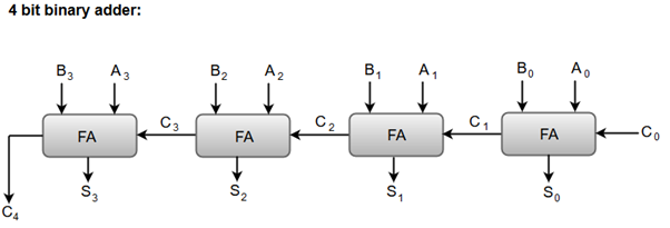
Binary AdderThe Add micro-operation requires registers that can hold the data and the digital components that can perform the arithmetic addition. A Binary Adder is a digital circuit that performs the arithmetic sum of two binary numbers provided with any length. A Binary Adder is constructed using full-adder circuits connected in series, with the output carry from one full-adder connected to the input carry of the next full-adder. The following block diagram shows the interconnections of four full-adder circuits to provide a 4-bit binary adder. 
Next TopicBinary Adder-Subtractor
|
 For Videos Join Our Youtube Channel: Join Now
Feedback
- Send your Feedback to [email protected]
Help Others, Please Share


